This thread has been locked.

If you have a related question, please click the "Ask a related question" button in the top right corner. The newly created question will be automatically linked to this question.

DRV8350S-EVM: High-side gate charge glitch and GDUV fault

Part Number: DRV8350S-EVM
Other Parts Discussed in Thread: DRV8350

Hi,

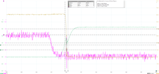
During the verification of our last design based on DRV8350S-RTV, we have observed that a combination of >44 V DC bus and a positive phase current (current leaving the drive towards the motor) causes a glitch in the phase voltage that seems to come from a drop in the High-Side gate voltage right after its rising edge.

When the current increases, the glitch gets as big as this

If an even greater current is demanded, commutation stops, and the gate driver reports a GDUV fault.

Then, apart from its clear relation to greater voltage and current, we have observed the following:

  • The higher the PWM frequency, the deeper the glitch is. The product uses 4 PWM frequency presets: 20 kHz, 50 kHz, 100 kHz, and 200 kHz.
  • Happens in 6x PWM mode and gets worse in Independent PWM mode (we use the second).
  • With a longer deadtime it gets slightly worse. When there exists a small beginning of a shot-through the glitch almost disappears (obviously not a solution).
  • Lowering the IDRIVEP_HS down to 300 mA seems to be the only effective solution, but the slow charge is limiting the small our minimum ON time can be.

Our hypothesis is the charge pump is not able to sustain a sufficient voltage during the charge of the high-side, but we don't have a clear explanation why. Although the VCP capacitor is 1 µF, 25 V, X7R, and the charge-pump switching node capacitor is a 47 nF, 100 V, X7R, following the datasheet recommendations, and the VM is supplied with 9.4 V, the high-side voltage decreases with the DC bus voltage and the magnitude of the positive current, reaching levels as low as 4.5 V and even less.

We would deeply appreciate any help on this topic, willing to complement this info with any other data you may require.

Thanks. 

  • Hi Ignacio ,

    Thanks for posting your question to the e2e forum - 

    The team is out of office for holiday timeframe, and will return to office on 1st week of January.

    We will try to investigate this behavior around then and provide a response with suggestions/feedback on your described problem 

    Best Regards, 
    Andrew

  • Hi Ignacio, 

    Thanks for your patience on this matter - 

    I have reviewed the information and have some feedback to help explain the behavior you're seeing on your system:

    1. In the case where you are seeing this HS Vgs behavior (voltage sag/dips during higher IDRIVE load),
      1. Question1: Are you seeing this on the DRV8350S-EVM (TI official EVM) itself, or is this data collected from your own system design based on our EVM? 
        1. just want to get an idea of whether layout might be a root cause here 
    2. The behavior you are sharing makes sense, and there are a few common root causes for this
      1. the suspected root cause is indeed the charge pump current capability in providing current for the gate drivers to operate 
        1. when the charge pump voltage is impacted, you'll see the HS Vgs and LS Vgs voltages also impacted as a result 
        2. this then goes on to impact your phase outputs SHx at the power stage, if the MOSFETs cannot switch properly
      2. the charge pump capability is impacted by your systems' DC bus voltage (aka VM)
        1. VCP can supply up to 25mA of average gate drive current to the MOSFETs. This gets lower if your VM is reduced, like you observed 
        2. the amount of current you'll need in your system is related to the peak IDRIVE setting, MOSFET Qgd spec, switching frequency, and # of FETs/gates 
        3. as you see in your results, the gate voltage dips are more severe when the load on the charge pump is too high 
      3. the charge pump effectiveness can be impacted by the charge pump capacitors and layout 
        1. for example, if your caps suffer from voltage de-rating then their effective value will be reduced. 
          1. I think your caps selected in the info provided should be okay though
        2. layout also has an impact. If your caps are very far away from the DRV device or are impacted by parasitic inductance from going through vias or narrow PCB traces, then their effectiveness will be reduced. We advise that any caps for the DRV device should be placed as close as possible to the IC, with proper thick traces (15 mils) and PCB 'teardrops' while also being on the same PCB layer as the DRV device (no vias in the signal path). 
      4. the gate drive performance is also impacted by gate drive traces
        1. ideally, you want to avoid having very long traces between DRV device pre-driver outputs and the MOSFET gate inputs 
        2. also want to use thicker gate drive traces to avoid parasitics. We advise 15-20 mils thickness
        3. also avoid going through multiple PCB layers (vias impact signal integrity) with these traces

    Charge pump current capability for average current scales down with lower VM voltage 

    Snippet of info from Smart Gate Drive app note: https://www.ti.com/lit/an/slva714d/slva714d.pdf

    Additional resource on best practices for board layout, and high-power motor driver PCB design: 

    Best Regards, 
    Andrew

  • Hi Ignacio, 

    Also, just to follow up on some of the other items discussed: 

    • With a longer deadtime it gets slightly worse. When there exists a small beginning of a shot-through the glitch almost disappears (obviously not a solution).
    • Lowering the IDRIVEP_HS down to 300 mA seems to be the only effective solution, but the slow charge is limiting the small our minimum ON time can be.

    What's the current rise time that you have? 

    • from the waveforms provided, it looks like T_rise is under 100nSec at the moment, which is very aggressive timing
    • if there are spikes in your gate drive waveforms (GHx, GLx, SHx) then you may want to take a look at the links below 
    1. Something that can be done to improve ringing at SHx would be to add RC snubbers parallel to HS and LS MOSFETs. 
    2. Gate drive signal ringing may be inherent to IDRIVE settings that are more than what's meant for the MOSFET's particular Qgd

    Smart Gate Drive app note: https://www.ti.com/lit/an/slva714d/slva714d.pdf

    IDRIVE setting selection: https://e2e.ti.com/support/motor-drivers-group/motor-drivers/f/motor-drivers-forum/796378/faq-selecting-the-best-idrive-setting-and-why-this-is-essential

    Please let us know if this information answers your questions, and if you require any additional assistance. Thanks!

    Best Regards, 
    Andrew 

  • Hi Andrew,

    Thanks a lot for such a complete and rigorous answer. I had to leave the project for some weeks, but now I'm back on track. Let me copy-paste your qüestions and try to respond to them one by one:

    I have reviewed the information and have some feedback to help explain the behavior you're seeing on your system:

    1. In the case where you are seeing this HS Vgs behavior (voltage sag/dips during higher IDRIVE load),
      1. Question1: Are you seeing this on the DRV8350S-EVM (TI official EVM) itself, or is this data collected from your own system design based on our EVM? 
        1. just want to get an idea of whether layout might be a root cause here
          • I'm measuring over our self-designed and manufactured PCB where the DRV8350S-RTV is included. I'm sorry for the confusion, I selected the DRV8350S-EVM because no other option was available from the forum web form. We do not have either have tested in the past the evaluation board.
          • The layout could be the root cause (though I would say we are pretty experienced in routing this kind of systems), and I can send further information for your evaluation through private channels if you believe it's gonna help us solve the issue.
    2. The behavior you are sharing makes sense, and there are a few common root causes for this
      1. the suspected root cause is indeed the charge pump current capability in providing current for the gate drivers to operate 
        1. when the charge pump voltage is impacted, you'll see the HS Vgs and LS Vgs voltages also impacted as a result 
        2. this then goes on to impact your phase outputs SHx at the power stage, if the MOSFETs cannot switch properly
          • Understood
      2. the charge pump capability is impacted by your systems' DC bus voltage (aka VM)
        1. VCP can supply up to 25mA of average gate drive current to the MOSFETs. This gets lower if your VM is reduced, like you observed 
          • In our design, VM is NOT connected to the DC bus (VDRAIN). VM receives 9.4 V from an on-board DC/DC (with 10 µF, 35 V, X7R as output capacity + 100 nF, 25 V, X7R right next to the VM pin). The DC bus is rated up to 60 V.
          • What I observed is the glitch understudy getting clearly deeper with the increase of the DC bus. In fact, it does hot happen under 43 V (tested with a light phase current of 1 A leaving towards the motor).
          • What is obviously relevant is the fact we are limited to only 10 mA VCP by having a 9.4 V supplying VM. The MOSFET's Vgs is rated 20 V (max. absolute), so I think we can try to increase VM a bit to see if this solves the issue.
        2. the amount of current you'll need in your system is related to the peak IDRIVE setting, MOSFET Qgd spec, switching frequency, and # of FETs/gates 
          • Limiting the HS source gate current does help. However, to get rid of the glitch at max current/max voltage we have to decrease it down to 300 mA, which is acceptable but not desirable (I can work with this, but I'd like to improve this number).
        3. as you see in your results, the gate voltage dips are more severe when the load on the charge pump is too high
          • Being the max. VCP current AVERAGE explains why it is clearly proportional to the PWM frequency. 
          • However, I still don't get why this does not happen to the low-sides. Could it be related to the fact that the HS gate "steady-state" voltages decrease when the DC bus voltage increases, getting as low as <5 V, while the low-side gate voltages remain barely modified? Could increasing the VM voltage help here too?  
      3. the charge pump effectiveness can be impacted by the charge pump capacitors and layout 
        1. for example, if your caps suffer from voltage de-rating then their effective value will be reduced. I think your caps selected in the info provided should be okay though
          • Does the recommended values of 47 nF and 1 uF consider any DC bias, thermal or aging derating?
        2. layout also has an impact. If your caps are very far away from the DRV device or are impacted by parasitic inductance from going through vias or narrow PCB traces, then their effectiveness will be reduced. We advise that any caps for the DRV device should be placed as close as possible to the IC, with proper thick traces (15 mils) and PCB 'teardrops' while also being on the same PCB layer as the DRV device (no vias in the signal path). 
          • I hope the following capture is self-explanatory:
      4. the gate drive performance is also impacted by gate drive traces
        1. ideally, you want to avoid having very long traces between DRV device pre-driver outputs and the MOSFET gate inputs 
          • The longest trace (CPH) is 2.2 mm.
        2. also want to use thicker gate drive traces to avoid parasitics. We advise 15-20 mils thickness
          • These 2 traces are 0.3 mm thick. Bottom and Mid-8 layers' copper are 42 µm (1 oz) separated by 65 µm prepreg.
        3. also avoid going through multiple PCB layers (vias impact signal integrity) with these traces
          • As seen in the previous image, both go through Mid-8, immediately under BOT layer.

    Also, just to follow up on some of the other items discussed: 

    What's the current rise time that you have?

    • from the waveforms provided, it looks like T_rise is under 100nSec at the moment, which is very aggressive timing
    • if there are spikes in your gate drive waveforms (GHx, GLx, SHx) then you may want to take a look at the links below 

    The phase rise time can be as low as 5 ns. The LS gate rise time is certainly a bit below 100 ns. The HS, I'm not sure about it, because the resolution is very bad due to the fact I'm referencing the measurement to GND, and thus subtracting the phase voltage from the gate voltage, which leaves only a few effective ADC bits.

    I'm trying out several gate current configurations, including all maxed, to decide where to put the limit.

    1. Something that can be done to improve ringing at SHx would be to add RC snubbers parallel to HS and LS MOSFETs. 
      • We typically try to avoid snubbers as much as possible. This product targets a very high level of miniaturization yet at the same time must be very efficient. RC snubbers are bulky and, essentially, energy dissipators. We will only include them as a last resource.
    2. Gate drive signal ringing may be inherent to IDRIVE settings that are more than what's meant for the MOSFET's particular Qgd

    So, there is a lot of very valuable information in the documents you linked, thank you very much. I'll try to focus on:

    • Evaluating the suitability of our maximum IDRIVE settings
    • Increasing the capacity of the charge pump capacitors
    • Increasing the VM voltage

    If any of those eventually solve the issue, I'll come back to you (it may take a while). 

    Best regards,

  • Hi Ignacio, 

    Sounds good, and thanks for your detailed response!

    I'm still catching up on the recent influx of e2e threads assigned to our team, so it may take me a few more days to review it in full for your ongoing questions. 

    For now, I do think these two are your best bets to improving the system performance 

    • Evaluating the suitability of our maximum IDRIVE settings
    • Increasing the VM voltage

    May want to avoid this one (the reason is that the capacitor values in datasheet were selected to match what the charge-pump regulator switching circuit can support across operating conditions. circuit charges flying cap and then transfers that stored charge to the storage capacitor. If cap values change, then it might not be guaranteed that the VCPH voltage can maintain the necessary value for gate-drive voltage to operate properly) 

    • Increasing the capacity of the charge pump capacitors

    Thanks and Best Regards, 
    Andrew 

  • Hi Ignacio,

    Very impressive rise time and frequency ringing at around 450Mhz, I did not know it was possible to switch power Mosfets so fast.

    I would check voltage on VCP pin, how it behaves when problem happens.

    "What is obviously relevant is the fact we are limited to only 10 mA VCP by having a 9.4 V supplying VM. The MOSFET's Vgs is rated 20 V (max. absolute), so I think we can try to increase VM a bit to see if this solves the issue." - worth of trying, increasing gate voltages would additionally lower RdsOn of Mosfets and lower conductive losses.

    "With a longer deadtime it gets slightly worse" - it could suggest that problems are related to Mosfet body diode reverse recovery and ringing caused by that phenomena. 

    I would also check voltage waveforms on INx pins against GND pin if there is no significant noise when problem happens.

    There is significant ringing at around 450Mhz, if I had a handheld 70cm 5W radio I would check if it causes any issues by transmitting with antenna close to PCB. Maybe it is not very scientific method but sometimes it allows to find problems with electromagnetic immunity.

    Regards,

    Grzegorz 

  • Hi Grzegorz, 

    Thanks very much for the added inputs on this! 

    We are glad to see e2e forum community engagement on debugging motor drivers

    Best Regards, 
    Andrew 

  • Hi Ignacio, 

    Appreciated on your patience from this - I did get a chance to review the information that you sent over, and have the below new comments:

    1. understood that you have your own personalized layout, which is different from the TI EVM examples
      1. in this case, we will need to look at your layout (thanks for attaching this up front) 
    2. VM=9.4V, as mentioned, so there's definitely an opportunity here to experiment with higher VM to improve average IDRIVE as mentioned
      1. please try this out and let me know if you see better results 
      2. for your other question, VGHS and VGLS are actually two different regulators
        1. VCP charge pump references Vdrain voltage
        2. VGLS references 0V GND typically, and I believe this is an LDO 
      3. increasing VM should help both regulators, including the LS, for gate-drive current as shown in the datasheet electrical table 
    3. Datasheet capacitor selection 
      1. We recommend that you use exactly the suggested values listed in the datasheet 'external components' section - as deviating from the standard values can cause the device's many regulators to be unstable
      2. to handle de-rating, we firstly account for this by selecting well-rated components
        1. DC voltage de-rating can cut the effective capacitance down to half, so we ask that you select capacitors that are rated for 2x the voltage they are expected to endure. Should go by at least** the voltage ratings listed in the 'recommended' column of Table21. 
        2. Similarly, temperature can de-rate your components as well -> so we suggest X5R or X7R to handle that appropriately. 
    4. Layout
      1. cap placement closeness looks good from initial glance 
        1. we also advice having sufficiently thick traces and 'teardrops' between the cap footprint and the DRV IC
      2. gate drive traces of 0.3mm = 12mils, if I am converting this correctly.
        1. For your use case, because you are experiencing problems, this is one of the first things I'd revise. 20mils thickness will help your gate drive capability a lot, especially for your system's aggressive switching rise time. 
        2. please also consider removing the vias from the gate drive path, and keep all gate drive signals on the same layer as DRV IC if possible. This would be my secondary priority recommendation 
        3. the reasoning for the two changes above is that thin traces and vias both add parasitic inductance, reducing the effectiveness of your gate drive current -> so the pre-drivers pull much more current to do the same job of turning the MOSFET gates on/off (this pulls your HS/LS regulator voltages down, as mentioned before) 

    As a final note: I am not too sure why the HS tends to do better than the LS pre-driver in our customers' reported findings, but I feel that there might be a reasonable explanation for this that is generic to half-bridge pre-drivers. I'll look into this and report back w/ any news I discover later.

    Thanks and Best Regards,
    Andrew

  • Hello again,

    I have progressed in the implementation of the items previously set, and got to what I think could be a dead end. Specifically:

    • Charge pump capacitors: disobeying your recommendations, I tried out changing the VCP-VDRAIN and the CPH-CPL capacitors.
      • My intention was to emulate a capacitor less affected by a DC bias derating, so I increased the recommended capacity by a factor of x1.5 approx. I tried increasing each separately, and then both at the same time, but could see no improvement.
      • Then I tried with a capacitor in the order of x0.5, but only for the CPH-CPL capacitor. Again, I could see no difference, which gives me a clue the problem is definitely not a lack of charge in the charge pump output.
      • Finally, I thought the problem could be in the frequency response of these capacitors, so I added a second, 1 nF NP0 capacitor in parallel to each one (right on top to minimize inductance, 0603 footprint). Again, I could see no improvement.

    • Increase the VM voltage to enable greater charge pump average output current: did not work at all. I previously had 9.4 V, to which a limitation of about 10 mA was assumed. With the changes implemented, I now have a voltage of 12 V, to which I expected a limitation of around 20 mA. Although I'm aware that even doubling the average current available could be insufficient for my transistor's gate charge when switching at 200 kHz, the thing is I did not notice any improvement at all:
      • VM = 9.4 V, positive current of a nominal magnitude, 60 V, 200 kHz, IDRIVEP_HS = 500 mA
      • VM = 12 Vpositive current of a nominal magnitude, 60 V, 200 kHz
      • VM = 9.4 V, positive current of a peak magnitude, 60 V, 200 kHz, IDRIVEP_HS = 400 mA
      • VM = 12 V, positive current of a peak magnitude, 60 V, 200 kHz, IDRIVEP_HS = 400 mA

    The last 2 cases are very close to the limit. Any further phase current or any further step in the HS gate current would trigger a gate driver fault. I implemented an SPI retrieval of the fault code and found a couple of cases and responses: VDS_OCP seems to be the typical error (changing the phase or transistor from board to board), more or less regardless of the Peak Gate-Current and the Over Current VDS level, but increasing the OCP deglitch time seems to change the reported error to GDUV.

    I'm not sure how to read this behavior... Maybe the phenomenon is the same, but allowed to perpetuate long enough get to cause a GDUV-like scenario? In any case, I measured the phase current, and I'm pretty sure there is no overcurrent in there. But could the overcurrent be actually caused by a cross-conduction (shot-through) small enough to not be destructive, and this be caused by a very weak self-activation of the low-side? I'm trying to make up a sort of hypothesis.

    In any case, I've got the feeling the issue is not going to get solved by working in the current direction. I don't think the problem is the charge pump output anymore, but more likely the activation of an HS strong pull-down or even the HS sink channel for some reason.

    Does it make any sense to you? Is there any High-Side gate built-in protection that would remain active in the Independent PWM mode, and that could behave in such a way? In this case, could it be related to the Low-Side?

    It doesn't go unnoticed to me that the rising edge of the phase voltage goes hand in hand with a severe ringing of the LS gate voltage that, in the more extreme cases, crosses the transistor's Vth. However, due to the instrumentation I'm using (spring ground as a return in the oscilloscope probe), I cannot completely trust the amplitude of this ringing. Although it is already rather small, I will try to minimize the inductance of the probe return even more.

    In any case, as I said earlier if no way to improve these 300 mA is found I'll just keep this value as a maximum and move on.

    Thanks,

  • Hi Ignacio, 

    Thanks for the follow-up in this case, and I will review this information further and try to get you a more detailed response by early next week. 

    Glad to hear that at least the project can move on even with 300mA, but I'll definitely do my best to answer your latest questions on potential root causes. 

    Best Regards, 
    Andrew 

  • Hi Ignacio,

    If you take a look a the last two waveforms you can notice that rising edge of LS Vds voltage in its steepest part rises by around 35V in around 2ns (zooming that area would help to estimate rise time better) what gives us around 17V/ns slope. The maximum recommended "Switch-node slew rate range (SHx)" is 2V/ns according to 7.3 table in datasheet. HS gate drivers and probably a couple of more circuits are referenced to SHx voltage inside DRV8350 and may malfunction if SHx voltage slope is too steep.

    Regards,

    Grzegorz

  • Hi Grzegorz,

    That's a wise appreciation, and I'm aware that we are trying to push the limits a bit with this product.

    To your more than reasonable concern, I'll point out that this product is intended to typically work along with way more relaxed slopes. I'm just trying to find the edge, and investigate the degree to which this Si-based power stage can satisfy a GaN-targeted application.

    Thanks and regards,

  • Hi Ignacio,

    Grzegorz makes a great point, this driver is intended to switch NMOS Power MOSFETs, which slew VDS voltages much slower than GaN-targeted applications. Too high of an SHx slew rate can result in electrical overstress. 

    Thanks,
    Aaron

  • Hi Aaron and Grzegorz,

    I just wanted to provide one last update before resolving the thread.

    These last weeks I've been performing a lot of tests for different sets of parameters (configurations) for my target applications, under the worst conditions I've been able to come up with:

    • Absolute maximum DC bus voltage
    • Maximum and minimum PWM frequencies (20 kHz .. 200 kHz)
    • Twice the maximum phase current (static, leaving and entering)
    • Twice the maximum phase current (commutation angle rotating at 100 Hz)

    In future tests, I will add temperature to those and try to endure some accelerated aging experiences to check for any lack of endurance or overstress.

    For the configurations obtained I had to reduce the HS gate current even more to 150 mA, which has indeed limited my duty cycle and thermal performance, but it is the only way I could ensure the GDUV / OCP error was not triggered along with the conditions stated above. Even if the resulting SHx rising slope is above 2 V/ns, I think the level of impact (and of gathered knowledge about this impact) this slope has on the various embedded protections and HS gate overall performance definitely admits future improvement. Not only I could reach a falling edge slope in the same pin about 3 times faster without ever noticing any sign of malfunction, but also I could try 1000 mA and 2000 mA gate currents to LS and HS sink (order of 10 times more) with no false fault reporting or critical distortion of the LS gate waveforms. 

    So, I measured the resulting rise/fall times for each configuration within 2 boundaries: the inferior being from 33% to 66% and the superior being from 2% to 98%. With this, the slowest slope in my slowest configuration ranges in dV/dt from 0.36 V/ns to 3.5 V/ns, and the fastest slope of my fastest configuration ranges from 3 V/ns to 18.2 V/ns. I know this is over specs, but I put these to the test and showed seamlessly stable performance. Regarding the duty cycles at 200 kHz (phase-to-phase DC bus utilization), the slowest configuration reaches 52 %, and the fastest is 82 % (painfully limited by those 150 mA in the rising edge).

    I leave a couple of captures to illustrate this:

    Wrapping this up, I think this is overall a satisfactory level of performance for a silicon-based power stage, especially having that most motor drives in the market are far from delivering at 200 kHz.

    Last but not least, let me guys thank you for your invaluable advice and support on this topic.

    Best regards,

  • Hi Ignacio,

    Thank you for sharing your experience and test results. It was very interesting to learn how fast power mosfets could be driven.

    Best Regards,

    Grzegorz

  • Hi Ignacio, 

    Thanks very much for sharing your latest results from the debug as well, and we'll keep this feedback in mind for our future debugs and new product developments.

    Best Regards, 
    Andrew