This thread has been locked.

If you have a related question, please click the "Ask a related question" button in the top right corner. The newly created question will be automatically linked to this question.

DRV8300: Custom board issues with DRV8300 & TMS320F28026F

Part Number: DRV8300
Other Parts Discussed in Thread: BOOSTXL-DRV8301, LAUNCHXL-F28027F, DRV8301,

Hi There,

I have been trying out the boostxl-drv8301 paired with the launchxl-f28027f to do FOC control with a brushless motor. It has been working great! I've been using example project 5h.

However, I've designed my own board with not quite the same chips, and having some issues. I think it's probably something simple missing with the gate driver.

  • Instead of f28027f MCU I am using f28026f which also has InstaSPIN enabled. 
  • Instead of DRV8301, I am using DRV8300, becuase the 8301 and other gate drivers are out of stock. (by the way, any idea when the 8301 will become available again?).

I've actually replaced the f28027f with a f28026f chip on the launchxl-f28027f eval board, and if works fine after changing the linker file.

On my board, I've added some external feedback circuitry that the 8300 does not provide. Other than that, the connections are pretty much identical to the two eval boards.

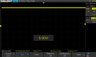
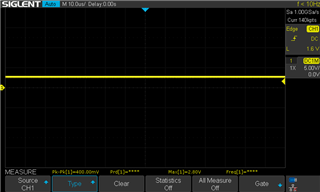
The problem I am having is that the gate driver isn't outputting anything. The bootstrap pins are at my supply voltage (16V), and I have tried a range of bootstrap capacitor values between 0.047uF to 10uF. But still, I seem to measure a voltage drop across the capacitors which would put the 8300 into UV lockout. BUT, maybe I'm measuring this wrong (without any outputs at expected frequency). Like I said, I've tried many cap values with no luck.

I have modified the user.h parameters to reflect my feedback circuit, and have verified that they work OK.

Other potential issue:

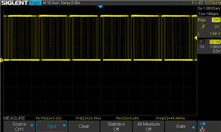
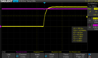
When I compare the PWM output signals on my board, to the eval board, there is a lot of transient noise in my signals... I can post a scope shot later. I'm wondering if this is preventing the 8300 from outputting anything, or if it's a result of no output at all.

When I run the program in debug mode and turn on the outputs, it goes into a run active mode like I would expect, but nothing happens on the gate driver side.

Any guidance would be much appreciated. Thanks!

Alec

DRV_MOTOR_DRIVER.pdf

  • Hi Alec, 

    Thanks for reaching out via our e2e forum!

    A few questions: 

    1. What does voltage look like on the GVDD pin? 
      1. is this pin also stable at 16V (same as PVDD?) 
    2. What is SHx voltage when you are seeing BSTx=16V?  
      1. are you seeing SHx voltage float up to 16V (same as PVDD?) 
    3. at INHx/INLx inputs, are you toggling these pins H/L using input PWMs? or holding it H always or L always? 
      1. based on your MODE pin setting (tied to GVDD), I expect the outputs to be inverted compared to your input PWMs. 
      2. toggling the inputs High and Low (through square wave / PWM) would confirm if pre-driver is OFF or is instead just driven Low 
    4. Also, devices with bootstrap-based architecture cannot achieve 100% duty cycle, 
      1. SHx needs to toggle low to 0V at least sometimes in order to provide HS gate-drive voltage. 

    Misc debug comments:

    1. in general, we recommend that every component show on the datasheet for '8.2 Function Block Diagram' is populated on your PCB. 
      1. Datasheet section '9.2 Typical Application' is also useful for this 
    2. Refer to section '9.2.2 Bootstrap Capacitor and GVDD Capacitor Selection'
      1. the GVDD cap needs to be at least 10x C_BSTx cap value 
      2. GVDD cap also should be rated for 2x or more of nominal voltage (e.g. 32V in your case) 
      3. I see C5,C6 placed on PCB by the MOSFET power stage for PVDD
        1. although your PVDD/GVDD are connected, GVDD needs its own cap placed closed to the DRV device to ensure bootstrap circuit operation over time 

    Hope the above information helps, and gives a good starting point for the debug. 

    Let me know if you have any further questions

    Thanks and Best Regards, 
    Andrew 

  • Thanks for the quick response Andrew. To answer your first questions,

    1. Voltage on GVDD pin is stable at 16.2V

    2. When BSTA is at 15.6V, SHA is at 2.8V w/ 0.1uF bootstrap capacitors (I can't seem to get this any higher with other cap values...)

    -both are "stable"

    3. for input PWM, I'm just using the defaul example FW which seems to be spitting out reasonable signals, besides the noise mentioned

    I will try PWM from external signal generator to confirm

  • BSTA:

    SHA:

    INHA:

  • Hi Alec, 

    Will review this info further tomorrow & aim to provide a response by early next week at latest. 

    Best Regards, 
    Andrew 

  • Thanks Andrew.

    Another interesting note: 

    With still no luck, I attempted to inject a square wave signal from an external sig gen into INHA. Nothing was seen on SHA. BTSA was at the supply voltage, GHA at the supply voltage, and GLA hanging out around 0V.

    However, I shorted together INHA and INLA, at which point a waveform with peak voltage near the supply voltage (16V) was produced on the GHA and SHA outputs, and the FET started switching successfully, the motor made strange noises. Of course because I this was not a valid signal for a 3-pwm configuration, and the other two channels were not active, I was not expecting the motor to do anything useful. But it does show that at least part of the circuitry is working OK.

    I have some concerns about the firmware I am running, because it's the example firmware built for interfacing with the DRV8301. It is indeed producing what seem to be valid PWM outputs on all channels, with channels A, B, and C offset 120 degrees in phase, but because nothing is happening on the driver side, it's stuck in a loop trying to get the feedback circuitry to respond. So, it changes the duty cycle of the waveforms between near-0% and near-100%.

    Despite my concerns, I would still think that the PWM signals should make the FETs switch regardless of whatever secondary issues I may have with the setup of the software fdbk parameters, and there is more than enough time for the bootstrap caps to charge up.

    - My PWM signals look very clean after switching to the "hardware verification" example of the FW.

    Another note on layout:

    My layout has the bootstrap capacitors placed pretty far from the chip. I understand the recommendation, but could this actually be affecting things?

    I have a 10uF cap placed as a bodge, close to the chip between GVDD and GND.

    Also, all caps in the gate drive circuit are rated at 50V

    I appreciate your help. If this turns out well, I should be placing large orders of the chips in the future.

    Thanks,
    Alec

  • Hi Alec, 

    Thanks for the updated response - 

    A few comments to help w/ debug: 

    • Would not advise shorting INHx/INLx together, as this can cause shoot-through to occur at the MOSFETs (both HS and LS FET on at same time means low-resistance path between DC-bus and GND, resulting in high current). This will damage the MOSFETs. 
    • The DRV8300 device only supports 6xPWM mode, I believe - so I would not suggest relying on the DRV8301 firmware too heavily, especially if it's expecting 3xPWM mode commutation logic. Agreed w/ your points about evaluating at level of checking square wave inputs vs output signals. 
    • I'd also advise checking BSTx vs SHx voltage differential during SHx switching, to verify that there is sufficient voltage 
      • this voltage differential needs to be between 5V and 20V at all times 

    Regarding Layout: (refer to section 11.2 of datasheet) 

    • yes bootstrap caps need to be close to the DRV IC for optimal performance 
      • this regulator circuit serves as overdrive voltage supply for the pre-driver outputs, meaning they're essential for the DRV IC to be able to produce +12V between HS/LS respective gate-source terminals. 
    • The GVDD cap is definitely essential for operation 
      • if I'm reading your comment correctly "I have a 10uF cap placed as a bodge, close to the chip between GVDD and GND"
      • does this mean you've 'blue-wire' soldered a cap connecting one end to GVDD pin and the other pin to GND? 
      • if so, then that should at least be a good temporary solution to experiment with. 

    Best Regards, 
    Andrew 

  • Hi Andrew,

    Thanks for the additional information.

    My SHX outputs are now within 2 to 3 volts of BSTX which is good, but they aren't switching with the PWMs.

    Yellow is the rising edge of PWM INH_A, and purple is SHA. You can see some effect on SHA, but it's not switching low.

    P.S. Yes, I am using 6 pwm. 

  • Hi Alec,

    Andrew is out of office today and he will be back tomorrow to answer your question!

    Thanks,
    Aaron

  • No problem, thanks.

  • Hi Andrew,

    I had the mode pin set to inverted rather than non-inverted. I'm all set I believe.

    Thanks much for your assistance.

    Alec