This thread has been locked.

If you have a related question, please click the "Ask a related question" button in the top right corner. The newly created question will be automatically linked to this question.

DRV8718-Q1: Undershoot issue on GH3

Part Number: DRV8718-Q1

Hi Team,

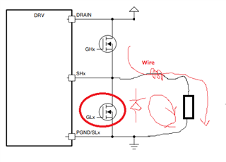
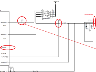
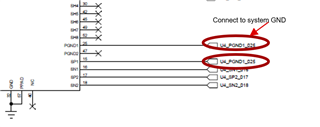
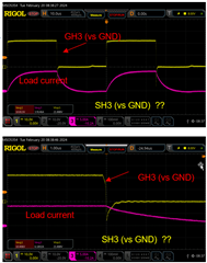
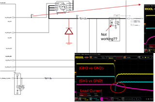
There is undershoot issue on GH3 when HB3_CTRL is controlled by PWM signal. Please check an attachment and let me know how to resolve or improve this issue, and please share it with me if there is a reference circuit.

240215_DRV8718Q1.pptx

Regards,

  • Hey Jeffrey,

    I have notified our experts on this device, please give them another day to get back to you on this.  Thanks!

  • Hi ,

    Thank you for your questions.

    Does customer use resistive load? What is the resistance?

    One key note is customer may need low side FET or diode even if resistive load. For gate driver usecase, normally load current is high (e.g >5A), then wire inductance is not ignorable.  We need diode path at low side for recircuration.

    Please double check whether customer has diode path. (D2 is mounted?).

    If D2 is mounted, please ask full schematic for DRV and external FETs. And need waveform for GH3, SH and current probe on resistive load (Zoom in like 10us/div and 1us/div). I guess GL3 is open. 

    Do they have only one GND on their PCB (All GND lines are connected)? Are they measuring waveform against only one GND? 

    regards

    Shinya Morita

  • Hi Shinya,

    Please check the customer's feedback below.

    Does customer use resistive load? What is the resistance? (Answer) Actually, I'm using a motor load. I used a resistive load for testing purposes.

    Please double check whether customer has diode path. D2 is mounted? (Answer) D2 is mounted.

    If D2 is mounted, please ask full schematic for DRV and external FETs. And need waveform for GH3, SH and current probe on resistive load (Zoom in like 10us/div and 1us/div). I guess GL3 is open. (Answer) I only control the High Side (use one FET), so GL3 is open. (PWM Control) Pleases review the schematic and waveform.

    Do they have only one GND on their PCB (All GND lines are connected)? Are they measuring waveform against only one GND? (Answer) Yes, I do, one GND.

    240220_DRV8718Q1.pptx

    Regards,

  • Hi Jeffry,

    Thank you for your feedback. 

    -I found PGND2 is OPEN. This should be connected to GND.

    -Where PGND1 is connected to?  Connecting to System GND?

    -As requested, previously, could you ask SH3 waveform as well?

    DRV has internal connection like bellow. If GH3 is gong to negative -15V like customer's waveform, SH should follow it. Then question is who drive SH3 to -~13V. If D2 does not exist, it could happen.

    Anyway, better to check SH3 voltage first.

    regards

    Shinya Morita

  • Hi Shinya,

    Please check the customer's feedback below.

    I found PGND2 is OPEN. This should be connected to GND. PGND2 is not connected to GND because the gate drivers of #5 to #8 are not used on their application. Please check it.

    Where PGND1 is connected to? Connecting to System GND? Please refer to the page 5 of updated attachment below.

    As requested, previously, could you ask SH3 waveform as well? Please refer to the updated attachment below.

    240221_DRV8718Q1.pptx

    Regards,

  • Hi Jeffrey,

    Customer's waveform tells us a lot of issue on their board. First of all, their SH shows -20V peak. This could damage DRV. Although they mentioned D2 diode is mounted, somehow D2 diode did not work. If diode works, SH voltage should not go below more than ~-0.7V by clamping of Vf. 

    They may need to put diode close to SH pin like bellow. Then this diode should handle >10A which is their motor current. (Or they can put same FET of HS at LS. Then LS external FET will have diode path)

    Again, DRV might be damaged already. I recommend replacing to new IC after adding high power diode (or LS FET) externally. 

    Even if CH5-8 are not used, I recommend to connect PGND2 to GND.

    PGND1 is a little complicated. Best way is use two HB form HB1-HB4 and one from HB5 to HB8. Because PGND1 is for HB1-4, PGND2 is HB5-8. However it requires significant PCB layout change. If customer can do this, this is simple configuration.

    If not, It is OK as is. Because HB3 use high side only, no problem PGND1 is connected to top side of current sense of HB1-2.

    regards

    Shinya Morita

  • Hi Shinya,

    Customer changed D2 diode to Schottky diode, -20V peak issue of SH has been improved like an attached waveform. Is it any problem?

    240223_DRV8718Q1.pptx

    Regards,

  • Hi Jeffrey,

    Looks good. Issue should be solved now. Please make sure customer will throw away all DRV which are damaged by -20V already.

    regards

    Shinya Morita