This thread has been locked.

If you have a related question, please click the "Ask a related question" button in the top right corner. The newly created question will be automatically linked to this question.

DRV8301: Gvdd is always zero volts

Part Number: DRV8301

Recently, we designed a motor driver. After power on, we found that the nFAULT pin reported an error. After reading the SPI controller, we found the GVDD_UV, then measure GVDD pin, found to be zero volt, excuse me, why this problem?

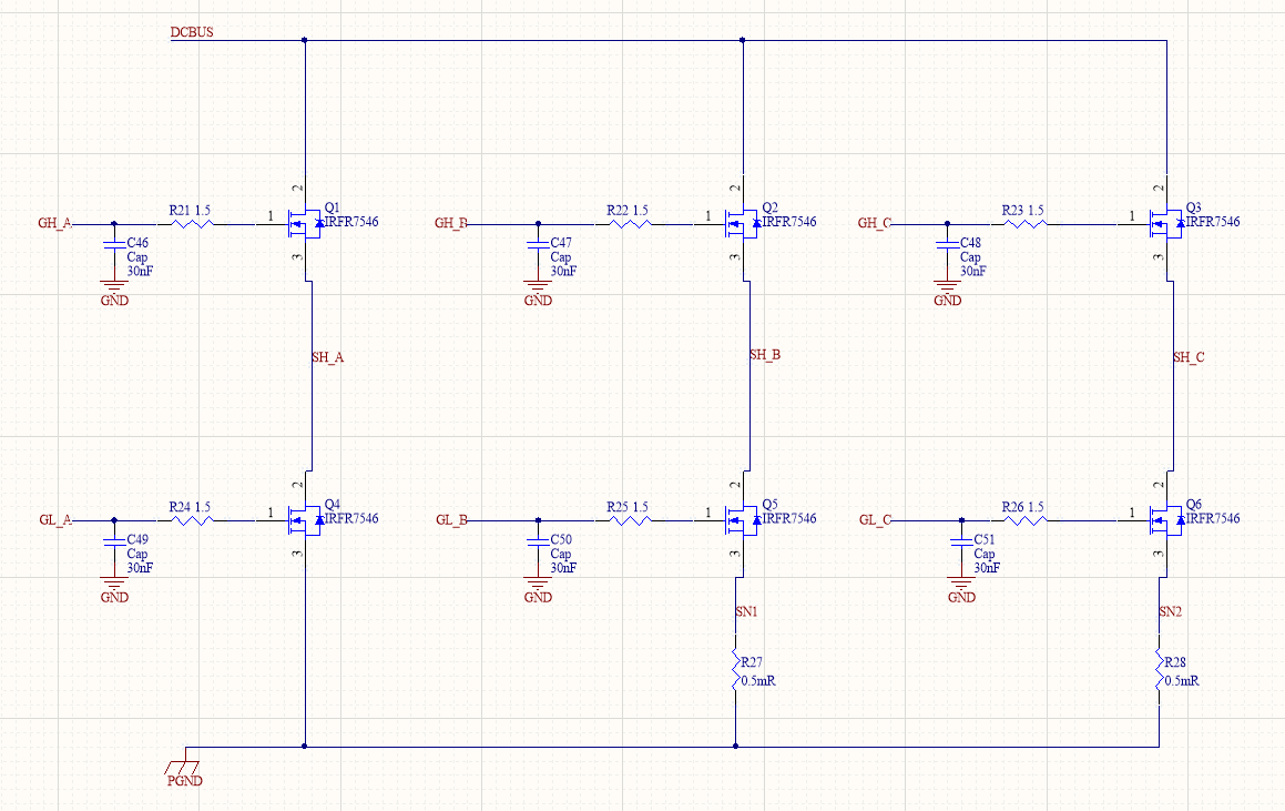
Here is our schematic:

The gate capacitor in the schematic is not welded

  • Hi Beyso,

    Thank you for posting your question in the MD Forum!

    I have a few questions to help get a better understanding of the situation:

    1. Did this issue occur the first time using the device? Or have you used this device or this design previously without any issues? I am wondering if there is any possibility that the device may have been damaged during previous use.
    2. Have you used a second device or PCB? If so, did it have the same issue?
    3. What is the DCBUS supply voltage that you are using to power the device?
    4. In your schematic you use PGND, AGND, and GND. Could you describe/show how these are interconnected?

    Thanks,

    Anthony Lodi

  • Hi Anthony,

    Thank you for your replying!

    1.When DRV8301 was soldering and powered on, this problem occurred. This batch of chips had not been used before. The design is modified according to the previous design. The original design has two PCB, which is connected through the pin, but it is not ideal. So we put the MOS and control part on the same PCB. The previous version of the design did not appear GVDD zero voltage.

    2.We have made a total of five PCBs in this batch, but now we have tested three PCBs and all of them have this problem

    3.DCBUS supply voltage is 12V.

    4.A single point connection is used on PGND,AGND and GND. Somewhere on the PCB, a small piece of copper is used to connect them together.

    Thanks,

    Beyso

  • Hi Beyso,

    Thank you for your response! Since you didn't have this issue on the previous design it is possible that the issue was caused by some of the changes that were made to the design. Can you summarize the changes you made, such as schematic changes, components selection changes, and layout changes? This may help understand what may be the causing the issue.

    Regards,

    Anthony Lodi

  • Hi Beyso,

    Do you have a pullup resistor on the nFault pin? since nFault is an open drain pin it needs a pullup resistor. I didn't see it on the schematic but you may have it near the MCU.

    Regards,

    Anthony Lodi

  • Hi Anthony,

    Thank you for your replying!

    There is a pullup resistor for the nfault pin. The schematic is as follows

    Compared with the previous design, the main changes are as follows:

    1. In the past, the control signals of MOS were connected by flying wires, but now they are connected by wires on PCB

    2. Previously, there was no pull-up resistance on the nfault pin. The design is as follows:

    However, the motor driver can still work normally and the LED will be on in case of an error. This seems to be in contradiction with the working principle of open drain output, but because it did not cause too much impact, we did not care about it too much.

    In addition, when we read the DRV8301 status register, we found that it reported GVDD_UV and GVDD_OV at the same time.

    Regards,

    Beyso

  • Hi Beyso,

    Thank you for the additional information! I have a few follow up questions:

    1. What gate drive current setting are you using for the device? This would be found in register 0x02, bits d0 and d1.
    2. Can you provide a waveform showing the voltage at the GVDD pin as well as the nFault pin (referenced to ground) prior to turning on the device, then turn on the device and monitor what you see on the oscilloscope?

    Regards,

    Anthony Lodi

  • Hi Anthony,

    Thank you for your replying!

    1.We use the default value, gate drive peak current 1.7A

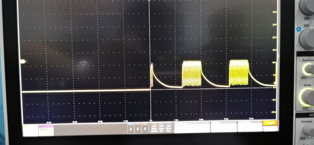
    2.This is the waveform of the nFAULT pin:

    This is the waveform of the GVDD pin:

    Regards,

    Beyso

  • Hi Beyso,

    Thank you for the waveforms!

    The gate drive setting you are using is really high for the IRFR7546. Because your MOSFETs have a low Qgd (18nC), The 1.7A setting will likely cause the MOSFETs to switch on and off too quickly, causing ringing and oscillation on the gate/source nodes which could be feeding back to GVDD, causing it to behave incorrectly. Can you try adjusting the gate drive setting to the lowest setting (0.25A) by changing D0 and D1 of register 0x02 to 01? Most customers consider 200nS to be a fast turn on time, and depending on the PCB design even 200nS could still be too fast. Even with the lowest setting for this device we still may need to increase the resistance of the gate resistors to slow down the gate current even more.

    Let me know if you notice a difference when using the lowest gate drive setting.

    You can also check out our IDRIVE FAQ page for more information: e2e.ti.com/.../796378

    Regards,

    Anthony Lodi

  • Hi Anthony,

    Thank you for your replying!

    After changing the gate drive setting to 0.25A, the GVDD waveform is as follows:

    There seems to be some change, but it's not significant

    This is the waveform of the gate control signal :

    But there is a strange thing, when we remove the gate resistance (equivalent to disconnect MOS), the gate control signal oscillation still exists.The waveform is as follows

    Thanks,

    Beyso

  • Hi Beyso,

    Thank you for your response! I have a few questions:

    1. Could you provide a waveform that shows PGND referenced to GND and AGND referenced to GND? If there is sufficient noise on the waveforms it may indicate that the grounds are not sufficiently connected to each other.
    2. What is the voltage rating for the CP1-CP2 capacitor, as well as the GVDD capacitor and the boot strap capacitors (BST_X-SH_X)?
    3. Could you provide images of your layout that show where these capacitors are located with respect to the pins of the DRV?
    4. When you are measuring the gate control signal, are you measuring from the high side gate to the high side source of the MOSFET? Or are you measuring from the high side gate to ground?
    5. The 1.5 ohm resistor may not be quite sufficient to slow down the switching time enough For this particular MOSFET even with the lowest iDrive setting. You may try using a 5-10 ohm resistor instead. It is also possible that the DRV could have been damaged when operating it at the 1.7A gate drive setting, so you may try to switch out the DRV and test it again with a new DRV while making sure the gate drive setting is on the lowest setting.

    Regards,

    Anthony Lodi