This thread has been locked.

If you have a related question, please click the "Ask a related question" button in the top right corner. The newly created question will be automatically linked to this question.

BQ76952: FET CHG cannot be controlled dependently

Part Number: BQ76952

Hi team,

Here's an issue from the customer may need your help:

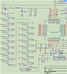
Design the board based on the chip manual and evaluation board related circuitry. Regarding the control of the FET, CHG and DSG cannot be controlled individually, issuing one of the instructions to the chip: DSG_PDSG_OFF, CHG_PCHG _OFF. The MOS tube cannot be controlled independently, the state is always jumping, and when the FET state is read, the state is always jumping and cannot be stable.

Could you help check this case? Thanks.

Best Regards,

Cherry

  • Hello Cherry,

    Do they have FET_EN set to 1? This is needed for most commands to work.

    Do they have a current going through the disabled FET? If current is going through the FETs while it is OFF, the body-diode protection feature of the IC can be triggered, turning the disabled FET on. This is explained in Section 5.2.3.1 FET Configuration of the Technical Reference Manual

    It may also be helpful to read this e2e thread which may explain how the commands work better: https://e2e.ti.com/support/power-management-group/power-management/f/power-management-forum/1051647/bq76942-write-fet_control-under-i2c.

    Best Regards,

    Luis Hernandez Salomon

  • Hi Luis,

    This issue has been resolved. Thanks. And here's also some additional question from the customer:

    1. The maximum Body DiodeThreshold of this register can be set to how many A? Do CHG and DSG have separate instructions to open?

    2. The self-developed board PDSG and PCHG are not properly controlled, and the two pins are not pulled high enough to control the MOS?

    3. What is the limit of the AFE transmit request? The test sends a request every 500 ms without problems, a problem occurs every 200 ms, and a problem occurs after 3 hours when a request is sent every 320 ms. The problem is that the individual voltage value and total voltage value cannot be read properly.

    4. A single cell cell battery balancing is always on during the test, and the balance threshold is set at 3400mV, and the actual battery voltage is around 3200mV, without exceeding the balancing threshold. Maybe because the MOS tube inside the chip is always closed, how to resolve this case? The chip-specific capture data plot is shown below: (Cell0 and cell1 are problematic)

    Thanks and regards,

    Cherry

  • Hello Cherry,

    Glad I could help.

    1. The maximum Body DiodeThreshold of this register can be set to how many A? Do CHG and DSG have separate instructions to open?
    The max threshold can be found in Section 13.3.3.11 Settings:Protection:Body Diode Threshold of the TRM. CHG/DSG would have the same threshold.

    2. The self-developed board PDSG and PCHG are not properly controlled, and the two pins are not pulled high enough to control the MOS?
    Could you elaborate better this? They should keep the VFETON of the Pre-charge/pre-discharge FETs to roughly 8-V. See Section 7.8 Precharge (PCHG) and Predischarge (PDSG) FET Drive of the datasheet.

    3. What is the limit of the AFE transmit request? The test sends a request every 500 ms without problems, a problem occurs every 200 ms, and a problem occurs after 3 hours when a request is sent every 320 ms. The problem is that the individual voltage value and total voltage value cannot be read properly.
    What values do they read when the errors occur? How often are they seeing the errors, do these error happen at a constant rate? It may be that the device and the host are not synchronized. Timing Requirements are mentioned in the datasheet.

    4. A single cell cell battery balancing is always on during the test, and the balance threshold is set at 3400mV, and the actual battery voltage is around 3200mV, without exceeding the balancing threshold. Maybe because the MOS tube inside the chip is always closed, how to resolve this case? The chip-specific capture data plot is shown below: (Cell0 and cell1 are problematic)
    Is internal or external cell balancing being used? Can they explain what is the data on the is being displayed in their picture? Maybe a picture of their schematic may be helpful.

    Best Regards,

    Luis Hernandez Salomon

  • Hi Luis,

    Thanks for your help again!

    The max threshold can be found in Section 13.3.3.11 Settings:Protection:Body Diode Threshold of the TRM. CHG/DSG would have the same threshold.

    The customer indeed would like to know if there are control instructions for DSG_PDSG_ON and CHG_PCHG_ON.

    Could you elaborate better this? They should keep the VFETON of the Pre-charge/pre-discharge FETs to roughly 8-V. See Section 7.8 Precharge (PCHG) and Predischarge (PDSG) FET Drive of the datasheet.

    PCHG and PDSG are measured using a multimeter. The voltage value VGS jumps between 43-45V. What should be the actual open voltage value of these two pins? Is this issue related to measuring method or the actual value is like this?  PDSG and PCHG are stuck open during the test. 

    What values do they read when the errors occur? How often are they seeing the errors, do these error happen at a constant rate? It may be that the device and the host are not synchronized. Timing Requirements are mentioned in the datasheet.

    Thanks, it dose due to the the synchronized issue and has been resolved by changing the way to read the voltage.

    Is internal or external cell balancing being used? Can they explain what is the data on the is being displayed in their picture? Maybe a picture of their schematic may be helpful.

    The figure shows the 16-bit data read by the 1- and 2-string battery chip. EA0 = 3744mV, FFFA value has overflowed. The actual hardware circuit measures the external balance resistance, resulting in voltages of 1.587 V and 3.724 V, and the actual battery voltage is around 3.2 V. From the number, it is because balancing is on, but now it cannot be turned off, and voltage data acquisition is abnormal.

    Thanks and regards,

    Cherry

  • Hello Cherry,

    The customer indeed would like to know if there are control instructions for DSG_PDSG_ON and CHG_PCHG_ON.
    I do not understand the question, those can be used to control the FETs.

    PCHG and PDSG are measured using a multimeter. The voltage value VGS jumps between 43-45V. What should be the actual open voltage value of these two pins? Is this issue related to measuring method or the actual value is like this?  PDSG and PCHG are stuck open during the test. 
    Are they measuring the gate to Vss or measuring the gate-source of the FETs? The gate-source voltage should be ~0-V if the FETs are off/open. In this older e2e thread I spoke some about how the tool impedance can affect the measurement to Vss: https://e2e.ti.com/support/power-management-group/power-management/f/power-management-forum/1067316/bq76952-i2c-communication-is-interrupted-and-the-sda-pin-is-pulled-low

    Thanks, it dose due to the the synchronized issue and has been resolved by changing the way to read the voltage.
    Good to hear!

    The figure shows the 16-bit data read by the 1- and 2-string battery chip. EA0 = 3744mV, FFFA value has overflowed. The actual hardware circuit measures the external balance resistance, resulting in voltages of 1.587 V and 3.724 V, and the actual battery voltage is around 3.2 V. From the number, it is because balancing is on, but now it cannot be turned off, and voltage data acquisition is abnormal.
    Does cell balancing occur during charging/discharging? Something that worries me, is the R34 1-Ohm resistor, why was this placed here? If the current is high enough, there could be a voltage drop here that I believe may affect measurements.

    Best Regards,

    Luis Hernandez Salomon