This thread has been locked.

If you have a related question, please click the "Ask a related question" button in the top right corner. The newly created question will be automatically linked to this question.

LM5116-HT: Cannot achieve an output/our mosfet not turning on

Part Number: LM5116-HT

https://e2e.ti.com/support/power-management-group/power-management/f/power-management-forum/1051689/lm5116-lm5116-design-review

Hi, 

I've just been asked by your customer support team to restart this thread here.  At the bottom is what I originally wrote.Since the first set of conversations with you, we had some new boards made using the high temp chip LM5116-HT and followed your layout guide, so there are some differences from before.  However, we still have not been able to get it to work.

As stated below, I'm assisting with this problem as Roger (design engineer) is away.  I'm able to send you any images/circuit designs you may need and do testing under your guidance.

We are really running out of time with this one and your quick assistance would be really really appreciated.

Happy to set up a call at anytime.

Jeff

+44 7771 767122

Hi there,

 Jonathan Navor was recently in discussion with my colleague Roger Jefferies regarding some problems we were having with your LM5116HJD chip. The ticket # was CS0750042 but the problem never really got resolved (out fault)

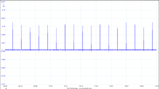
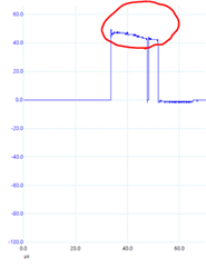
The enable is correct, as is the UVLO and the SS voltage. There is a ramp signal at around 105kHz. There is something at the Ho pin but it does not turn the MOSFET on.’

 Roger is currently away from work and i am assisting in working through the issue.  I have boards in my possession but I'm no expert (mechanical engineer..).  I can follow instructions and use a PicoScope, so i'm hoping we can make this work.

 I did re-send the conversation to our 'service-now' address, but thought it also wise to create a new ticket.  We have a fast approaching critical  deadline and I'm really hoping you can help.

Regards,

Jeff

  • Hi Eric. 

    We changed our MOSFET (Q5) to FDB390N15A. No change from previous results

    We then connected VCCX to ground.  All results the same as before except:

    Pin 10.  Was 126mV, now 0

    Pin 17.  Was 125mV, now 0 

    See below

    1 50.
    2 1.47
    3 1.22
    4 50
    5 288mV
    6 0
    7 266mV
    8 46mV
    9 5.5
    10 0
    11 0
    12 0
    13 0
    14 0
    15 40mV
    16 7.37
    17 0
    18 6.86
    19 4.11
    20 4

    Our MOSFET (Q5) is not switching on because there is no gate drive. Both Ho and SW are sat at approx. 4V. (19 & 20)

    Lo is a short duration pulse. Should this be switching the lowside MOSFET on, and for longer, thus pulling the SW output down, and giving a highside MOSFET a 4V gate drive?

    Also, what is the duration of the lowside MOSFET drive with the inductor removed?

    Thanks,

    Jeff

  • Hello Jeff 

    LO-GND pulse is short now because high-side switch doesn't turn on / it turns on but the inductor is disconnected.

    Once the high-side switch start switching and the inductor is reconnected,  the LO-GND / HO-SW duty cycle will  be determined by D=Vout/Vin in steady state 

    - Eric Lee (Applications Engineering) 

  • Hi Eric,

    We reconnected the inductor, but still it does not switch on. 

    What waveform would we expect to see on SW (pin 20) with the inductor removed/fitted?

    From any of the voltages I have given you, can you tell if the IC is damaged or not? 

    Thanks,

    Jeff

  • Hello Jeff 

    SW node voltage should be almost same as buck converter input voltage when the high-side switch turns on. 

    Since the VCC regulator is working and LO is switching, I don't think the IC is damaged now.  

    Please let me know once the high-side MOSFET starts switching. Please check the gate-to source voltage and all three terminal connections. 

    - Eric Lee (Applications Engineering)

  • Hi Eric,

    We decided to change the IC for the low temp version LM5116MH/NOPB using an adapter.  This time, we got different and better results.

    But, when we reconnected the inductor and slowly increased the supply voltage there was a lot of ringing from the IC and then the chip failed, we think at the point where the voltage crossed the UVLO.

    The load on the circuit was 0.

    What do you think

    55 1
    1.61 2
    1.21 3
    54.5 4
    289mV 5
    0 6
    350mV 7
    57mV 8
    5.45 9
    0.5 10
    0 11
    0 12
    0 13
    0 14
    43mV 15
    7.3 16
    1 17
    59 (pulses to 0) 18
    58 (pulses to 0) 19
    53 (pulses to 0) 20

    Thanks,

    Jeff

  • Hello Jeff 

    I'd like to see pin 18,19,20 waveforms (just 2-3 cycles in the same screen capture) if possible. 

    It is interesting that #10 pin is connected to #17 pin, but one pin voltage is 0.5V while the other pin voltage is 1V.  You should check if any trace is damaged. If the connection from #10 pin to the output and #17 pin to the output are okay, it means that your DVM is not working well. 

    If #20 pin voltage is 53V while #10 is 0.5V, that means trace is open or inductor is damaged. 

    - Eric Lee (Applications Engineering) 

  • Hi Eric,

    Apologies.  i may not have explained properly.  The voltages in the table are with the inductor removed.  We blow the chip as soon as then inductor is connected and (we believe) UVLO is reached.

    I will send waveforms later anyway.

    Jeff

  • Hello Jeff 

    Even if the inductor was removed when you measure the voltages, it doesn't make sense that #10 pin voltage is different than #17 pin voltage .

    - Eric Lee (Applications Engineering) 

  • Hi Eric,

    We repeated the tests, but with very similar voltages on pins 10 & 17.  This is strange as we did this test twice last week where pin 17 was 1V.

    Attached are results and waveforms. I have captured pins 18 & 19 together, 18 & 20 together and 19 & 20 together as i only have 2 ch scope.

    FYI, we are waiting on the delivery of a better scope.

    I really appreciate all your help so far.  Thanks!

    Jeff8 - TI - Feb 7th.docx

  • Hello Jeff 

    As you can see on the #19, #20 waveforms, the high-side MOSFET switches now.
    Next step is to connect the inductor. Before connecting the inductor, please set your power supply current limit to 0.2A and remove the load. 
    -Eric Lee Applications Engineering)

  • Hi Eric,

    I connected the inductor (47uH) and had no load connected.  The IC blew at around 42V which is around the UVLO point.  We briefly saw around 20V output on the meter and there was a lot of screeching from the IC.  Basically, the same results as last week.

    It is more difficult to set the current limit on the bench supply here, so will repeat tomorrow in the lab with a different supply, but I am expecting a similar result.  If we blow IC's with no load, there is still something very wrong.

    Thanks,

    Jeff

  • Hello Jeff

    Please set the power supply current limit < ~0.3A, then most of time there will be no damage. 
    Also, please increase Css (~ 10uF?) then you will be able to have more time to check the transient performance  

    - Eric Lee (Application Engineering) 

  • Hi Eric,

    Just to give you an update.  For some reason, we have gone back to the situation where we cannot get an output from the MOSFET.  This is similar to how things were before we started using the low temp LM5116MH/NOPB on an adapter.  This is despite trying two different chips and two different boards. As soon as we work out what is happening, I will get back to you.

    Regards,

    Jeff

  • Hi Eric,

    I'm not sure if my previous post actually got sent.

    We managed to get back to where we were (low temp chip), but also lowered (for testing purposes), the output voltage to 36V from 48V.  This makes the output voltage lower than the UVLO which is still at 42V.

    We got good numbers on the IC, but once again, blew the IC after the 47uH inductor was connected.  

    I have attached a trace from SW (pin 20) and the voltages obtained before the inductor was re-connected.

    Thanks,

    Jeff10 - TI - Feb 18th.docx

  • Hello Jeff 

    1. #15 pin voltage is wrong, or the device is damaged already.

    2. Please measure  #18 minus #20 voltage too. 

    3. Pin 20 waveform without inductor is normal

    4. Pin 20 waveform with inductor is abnormal. 

    -Eric Lee (Applications Engineering) 

  • Hello Jeff

    1. Please see the SW voltage drop when the high side switch is on. I see about 5V drop, which can be caused by 500A inductor current if the high-side MOSFET Rdson is 10mOhm.

    2. Based on your waveform,  the high-side MOSFET turns on for more than 10us, which is also not normal. 

    - Eric Lee (Applications Engineering) 

  • Hi Eric.

    i made a mistake with #15.  It should have been 47.2mV

    What could be the cause of the voltage drop and how do we resolve it?

    Thanks,

    Jeff

  • Hello Jeff

    At first, you have to check if your measurement is correct or not. Please measure inductor current.

    SInce 5V=500A x 10mOhm, Case1) your 5V measurement is wrong Case2) 500A is actually flowing into the inductor Case3) Your MOSFET Rdson is very high. Higher than extectation.  

    - Eric Lee 

  • Hello Jeff 

    Usually, such a big voltage drop is caused because the MOSFET gate threshold is too high, or the V(HO-SW) is not high enough to fully enhance the MOSFET.

    - Eric Lee (Applications Engineering) 

  • Hi Eric,

    Thanks.  The engineer is not available for a few days, but i will get him to look at this as soon as possible.

    Thanks, Jeff

  • Hello Jeff 

    Please let me know if any update

    -Eric Lee(Applications Engineering)

  • Hi Eric,

    Just to let you know that the engineer is back tomorrow.  Hopefully, we should have an update for you soon.  Thank you for your patience.!

    Jeff

  • Hello Jeff 

    Please let me know if any update

    -Eric Lee(Applications Engineering)

  • Hi Eric,

    Sorry for the delay.  The engineer has been trying a different approach.  We changed the ceramic capacitors (C7-C10) on our schematic for a 56uF wet tanatalum capacitor and added a 10uF cap in parallel across C11.

    We then dropped the UVLO to 30V and changed the output to 12V.  

    It worked, but when the output was then changed to 24V, we blew the chip again.  

    Please see the attached 

    Jeff04.docx

  • Hello Jeff 

    I'd like to suggest you to evaluate your system as much as possible at 12V since it works at 12V output. 

    1. Can you figure it out which component change helped ? C11 ? C7//8//9//10 ?

    2. Can you measure a loop response ? 

    3. Can you check if any overshoot at #1 and #20 pin ? 

    4. Inductor is saturating ?

  • Hi Eric,

    We will work through your questions and get you the answers:

    Also:

    1. You commented in an earlier post that Rds (on) for the highside switch is high, so today we are changing it for a lower value.

    Will a high Rds(on) value be able to blow the IC?

    2. The webench software gives a value of 2u2 for the supply decoupling, whereas the quick start spreadsheet states 20uF.

    Which value is correct and if we have fitted the lower value would that kill the regulator?

    Thanks,

    Jeff

  • Hello Jeff

    1. There is a possibility the IC got damaged at the same time when a MOSFET got damaged. 

    2.  Does the supply-decoupling mean the input capacitors of  buck converters ?

    3. I have a question. Have you ever studied the EVM layout / the layout guidelines of this device ?  

    - Eric Lee (Applications Engineering) 

  • Hi Eric,

    In answer to your recent questions:

    1. Can you figure it out which component change helped ? C11 ? C7//8//9//10 ?  We don't think the capacitor changes made any difference.

    2. Can you measure a loop response ? Unfortunately, we don't have facilities to measure the loop response

    3. Can you check if any overshoot at #1 and #20 pin ? .There is no overshoot on either pins #1 or #20

    4. Inductor is saturating ?. We don't think so.  It is a 5A device

    1. There is a possibility the IC got damaged at the same time when a MOSFET got damaged. The MOSFET was not damaged. It was replaced with one with a much lower Rds(on)

    2.  Does the supply-decoupling mean the input capacitors of  buck converters ? The capacitor was Cin on the Quickstart XLS, and C5 in our schematic.

    3. I have a question. Have you ever studied the EVM layout / the layout guidelines of this device ?  

    Yes, we supplied the layout guidelines to the PCB designer.  Did you spot anything unusual when you looked at our gerber files/schematic?


    We changed more components today and did some further testing, but still with a low output voltage.  Please see the attached.

    Thanks,

    Jeff05.docx

  • Hello Jeff

    A loop instability can be caused if the supply-decoupling capacitor is not enough, then the converter can be damaged by an oscillation due to the instability. Have you observed any inductor current oscillation ? 

    It is a normal waveform. During DCM operation, the SW node voltage rings due to a resonance. 

    - Eric Lee (Applications Engineering)  

  • 06.docxHi Eric,

    The engineer added a snubber to reduce overshoot.  Also, our inductor is 7A, not 5A as previously stated.  As before, when the output voltage is set low, all is OK, but as soon as it is increased (in this case to 24V), the IC fails. We just can't see why.

    Jeff

  • I am out of office now. I will reply as soon as possible when returning back

    - Eric Lee (Applications Engineering) 

  • Hello Jeff

    The transfer function of the feedback amplifier circuit including loop compensation components is affected by the Rfb2 resistor value. Rather than R29, please try to change R30. 

    - Eric Lee (Applications Engineering)

  • Hi Eric,

    So if the loop compensation is wrong, can this kill the IC?

    Regards, Jeff

  • Hello Jeff 

    Yes, it is possible to make a damage if the system oscillates. Usually, you can observe an inductor current oscillation or hear a high pitch noise if the system oscillates. I wish you can measure loop response.

    - Eric Lee (Applications Engineering)

  • Hi Eric,

    We changed R29 back to its original value (47K) and changed R30 to 5K (was 1K2).

    The input voltage was ramped up to 31V. The output came live at approx. 14V

     The signal an SW was clean

     The input voltage was ramped down to zero, then quickly ramped up to 30V. The output started to come live, but then the IC died.

     Another chip was fitted. The output came live, but was unstable. Then the IC died.

    Jeff

  • Hello Jeff 

    • If the issue happens by a fast toggling of the power supply, adding a small ceramic capacitor at the VIN pin might help. 
    • You said there is no overshoot, but it looks like it is better to double check if any overshoot when powering on your power supply. The overshoot can happen by a long input cable.

    - Eric Lee (Applications Engineering) 

  • Hi Eric, 

    Sorry for the long delay in replying.  We tried changing component values to a set of values copied from a working regulator design of a similar input/output condition and the regulator still failed to work.

    The only conclusion that we could come to was that there was an issue with the layout. A test board has been designed with a similar layout to the example in the TI data sheet. The board is now on order and will shortly be built and tested.

    Did you notice anything wrong with the layout we sent you at the start of this conversation?

    Also, there are two sets of design software, Webench and Quickstart..For the same input and output requirements there are different component values given depending on which package you use.  Which software is correct?

    Regards,

    Jeff

  • Hello Jeff 

    Please follow the components values from the QuickStart if any difference. 

    If you want, please share your QuickStart, schematic and layout for my review. 

    - Eric Lee

  • Hi Eric,

    Attached are the Quickstart, schematic and layout for the test piece.

    Regards,

    Jeff4604.GWK1.pdf6305.LM5116_quickstart.xlstest piece.pdf

  • Hello Jeff 

    Thanks for sharing the information. Please refer my comments below. 

    • Consider adding a diode and a capacitor at the UVLO pin. Please refer Functional block diagram
    • Use 0 ohm at R23. Increase the resistor value later when required
    • Use 390nF at C4
    • Input de-rated capacitor values at the cell E24 and E25. Effective capacitance is reduced by applied voltage
    • Double check R26 power rating
    • D13 anode trace is too thin
    • R54 and C27 should be placed close to Q6
    • #13 pin should be directly connected to the negative connection of R26. Use kelvin-connection
    • #6 pin should be directly connected to a large analog ground copper whose net name is '0VB'
    • #14 pin should be connected to #6 and a large power ground copper whose net name is 'GND'
    • Copper-pour "GND' net to all empty area on both top and bottom.

    -Eric lee

  • Hello Jeff

    • Make #19 to the high-side gate trace thicker
    • Make #15 to the low-side gate trace thicker
    • Please C12 close to the IC

    - Eric Lee

  • Hi Eric,

    We have implemented your comments as much as possible.  Revised schematic attached.

    Regards,

    Jeffregulator schematic.pdf

  • Hello Jeff 

    Thanks for sharing the information. 

    - Eric Lee