This thread has been locked.

If you have a related question, please click the "Ask a related question" button in the top right corner. The newly created question will be automatically linked to this question.

BQ78350: Schematic check

Part Number: BQ78350
Other Parts Discussed in Thread: BQ76920, , TIDA-00792, , BQ769200, TIDA-01093

Dear ,

Could you please help to check the circuits of several TI chips?

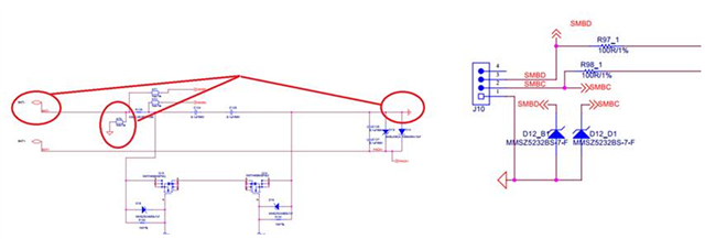
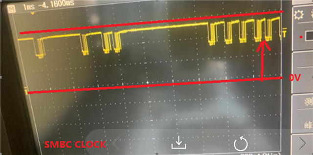
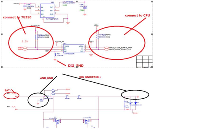
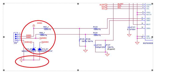
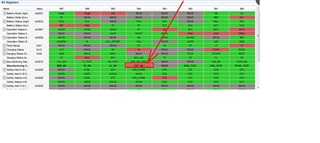
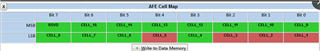
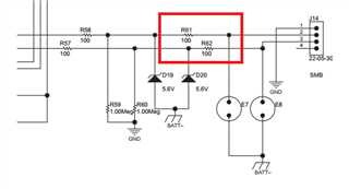
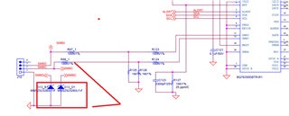
Especially for BQ79620 and BD78350, I measured that there is a 0.4V difference between analog ground and digital ground directly, and the following two diodes are easy to be damaged and burned, so I want to confirm whether the relevant circuit is correct?the schematic is attached as below ,many thanks

 yunhu-zhuban-v03.pdf

  • Hi Cooper,

    Is there a large charge or discharge current when the voltage difference is observed? What is the charging voltage applied to PACK+?

    Regards,

    Matt

  • HI Matt:

    I still hope to confirm the schematic diagram is correct before discussing specific problems. What I sent is the schematic diagram of the mother board, including BQ78350, BQ76920 and charging IC.

    For the voltage difference problem,

    I didn't connect the load, I just connected the four batteries to the motherboard,

    The motherboard, which converts four batteries into 5V and 3.3V, supplies power to the core board,

    Sub-board, CPU+PMU+MEMORY,

    Look at the circuit, PACK+ is connected to the positive electrode of the battery, PACK- is connected to the main ground of the system? The negative electrode of the battery is connected to the main ground of the system through two MOS.

  • Hi Cooper,

    I think the issue may be that you are referencing SMBD and SMBC to VSS (BAT-) when they should be referenced to PACK-. See TIDA-00792 for an example of how these should be connected. https://www.ti.com/tool/TIDA-00792 

    This thread gives some insight into why you want to reference PACK- on the comms: https://e2e.ti.com/support/power-management-group/power-management/f/power-management-forum/823905/bq76930-bat---or-pack---or-other-ways-to-connect-gnd

    A few other things I notice in your schematic unrelated to this issue:

    • The BQ78350 COM pin should not be connected if it is not used. See datasheet pin table.
    • The BQ78350-R1A is recommended (instead of the R1) for new designs. R1A comes pre-loaded with the latest version of the firmware.
    • The bottom of C118 should connect to GND (instead of to VC0). This shouldn't be a big problem though.
    • If you are using cell balancing, the Zener diodes (D17, D19, D20, D21) could cause issues since they are 5.6V.

    Best regards,

    Matt

  • Matt:

    Q1:

    Our first problem is shown in the figure below. There is a communication problem between CPU and BQ78350. We found that the low level of SMBC is higher than the normal range. The COMMUNICATION between CPU and BQ78350 cannot be guaranteed

    Q2;

    The following circuit, AND_GND and DIG_GND are connected according to the development board of TI BQ76920. If there is a voltage difference between the two GND (TI demo also has the voltage difference), how to ensure the communication between BQ78350 and the main chip?

  • Hi Cooper,

    I think I see your issue. U47 which communicates to the SMBus is referenced to PACK- but the BQ78350 and the diodes are referenced to BATT-. This will be an issue especially when the FETs open due to a protection triggering. If the FETs open, you will lose communication unless you have an isolator between these two devices. If U37 is inside the PACK, then it should reference the same GND as the other ICs.

    You are correct, the EVM does reference BATT- because it uses low-side FETs. The TIDA-00792 uses PACK- as a reference because high-side FETs are used in that design. 

    Best regards,

    Matt

  • Since there is no doubt about the schematic, let me talk about the specific problems。

    This project is a series of 4 batteries. When I measured the voltage value of SMBUS relative to DIG_GND on the device U47, I found that when 4 batteries are placed in the machine, SMBUS to DIG_GND is normal 0V,

    When one battery is removed and only 3 batteries are placed in the battery, the SMBUS is -2V(to -5V) to DIG_GND, and this negative pressure will cause damage to the conversion chip U47.

    My understanding is that the BQ73850 is not working properly when there is one less battery, so DSG_EN is not turned on. ANA_GND and DIG_GND are disconnected, but the MOS Q13 Q14 causes the GND on both sides to be connected, and a negative pressure state occurs.

    Questions are as follows,

    1. Is there a problem with the configuration of the BQ73850?

    2. How to solve the problem of negative voltage between two GNDs? ,

    3. Short-circuiting ANA_GND and DIG_GND directly can solve the problem of negative voltage, but is there any problem with this design?

  • Hi Yabin,

    If the BQ78350 is configured for 4 cells (AFE Cell Map register setting), then changing to 3 cells will likely cause the device to trigger under-voltage or a voltage-based Shutdown. 

    However, the DSG FET should open to protect the battery, so you want communication to still be possible even if the DSG FET opens. In this case you need some type of isolator chip for the SMBus or you can use high-side FETs so that the DSG FET opening does not disconnect the communications.

    Best regards,

    Matt

  • hi Matt,

    Yes, we plan to change the schematic later to use high-side FETs, but now we need to make corrections to the current version of the circuit.

    So like you said, now we have set 4 batteries, if only 3 batteries are placed, can BQ78350 actively turn off FET_EN? (We have FET_EN turned on in our settings, as shown in the picture) I have always suspected that there is a problem with our settings.BQ78350 configuration

  • Sorry, I meant to keep FET_EN on consistently, so that the levels of both GNDs can be kept the same.
    Alternatively, can you recommend a related isolator chip?
    Or what if I use flying leads to connect the two GNDs together?

  • Hi Yabin,

    Have you checked your setting for the AFE Cell Config register? This should reflect how many cell are connected.

    Regards,

    Matt

  • Hi Matt

    Do you mean, I set up 4 cells now, but I can turn on the MOS when preventing 1 cell, 2 cells and 3 cells, so that the two GNDs are connected together? Or it is necessary to add isolation devices to ensure that the negative voltage will not affect the circuit on the CPU side?I didn't find the registers, please provide the specific reg and documentation.
    And will this cause another problem, if I put 4 batteries, 1 battery is 2V (abnormal battery) and the other 3 batteries are 4V (normal battery), my understanding is that the 78350 should be disconnecting both GND , to ensure that the system does not boot. In this case, is negative voltage still unavoidable?

  • Hi Yabin,

    Search for the AFE Cell Config register in the TRM. Here is the document: https://www.ti.com/lit/ug/sluuc78/sluuc78.pdf 

    This register must be configured for the number of cells you are using. 

    Regards,

    Matt

  • Hi Matt

     I understand what you mean, I know this document and configure it according to this document. So after placing 4 normal batteries, the system is normal.

    But the problem is that a total of 4 batteries are connected in series, and the batteries are placed one by one. Therefore, when the battery is placed with 1, 2, and 3 batteries, the SMBUS line will have a negative voltage state on the GND on the CPU side. This negative voltage now seems to have damaged the U47 chip. So what I have been struggling with is how to prevent this negative voltage from damaging the chip.

    So the known measures are to use Plan1. use some type of isolator chip for the SMBus, Plan2, use high-side FETs. Is there any other solution?

    Since the EVM of the BQ769200 uses low-side FETs, there should not be such a problem of negative pressure causing damage to the device.

  • HI Matt,

    Please help us check the map settings. Do the settings in the picture correspond to the schematic? Weird, we think this is right, but in fact the software colleague told me that he can only read the voltage of VC1-VC2-VC3-VC4, but not the voltage of VC5

  • Hi Yabin,

    These settings are correct if 4 cells are connected. This specifies which pins of the BQ76920 monitor are connected to cells. If you remove one of the cells (set only 3 cells) and if you do not change these settings, then one cell will measure 0V - this will trigger an under-voltage fault (if under-voltage is enabled) and it will trigger a voltage-based Shutdown (see your register setting for the Shutdown voltage). An under-voltage protection will cause the DSG FET to open, Shutdown will cause both FETs to open.

    When the FETs open, you are losing the connection between your grounds.

    Regards,

    Matt

  • HI Matt。

    I found a circuit connection difference on the schematic, R61 and R62 in the reference design are 100ohm connected in series between the two systems, while our schematic puts two TVSs at the interface. Is it possible that this place caused the negative pressure to damage the CPU side? Is it possible to increase these two resistors to prevent damage to the CPU side interface?

  • Hi Yabin,

    As I explained earlier in this thread, there is an issue because U47 is referenced to PACK- and this will lose connection to BATT- when the FETs are disabled. So your CPU is losing its ground connection which is a problem. In this case, you will need to use an isolator device or use high-side FETs.

    Regards,

    Matt

  • Hi Matt,

    Got it, do you have a recommended isolator device?

  • Hi Yabin,

    TIDA-01093 (https://www.ti.com/tool/TIDA-01093 ) uses an isolator device on the I2C of one of the battery monitors. I am not too familiar with the isolator parts, so you may want to search on ti.com to see if there are newer options. 

    Best regards,

    Matt

  • This is exactly what I need, thanks