This thread has been locked.

If you have a related question, please click the "Ask a related question" button in the top right corner. The newly created question will be automatically linked to this question.

TPS65185: Design review

Part Number: TPS65185

Hi,

I had previously asked a question here about issues with a design involving the TPS65185 PMIC. However, my requirements changed slightly, so I am working on a revision to that design, and thought it would be better this time to ask for a review before getting the board fabricated...

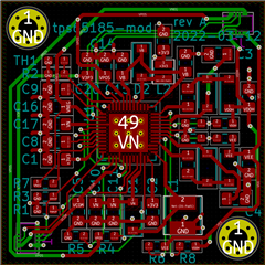
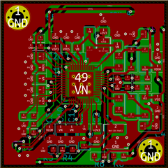
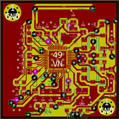
This time, I have put the TPS65185 and supporting circuitry on a module with two board-to-board connectors on the bottom, so that I can easily reuse the circuit in different prototypes. If possible, it would be great to get the design of this module reviewed. It is a four layer board, with a stackup of: signal layer and components (top), ground plane, 3.3V plane, signal layer (bottom). The top and bottom layers also have a ground fill where there's no signals. For the most part, I tried to follow what the reference design did in terms of routing.

I have attached the schematic to the end of this post as a PDF, and images of the PCB design are below. I have also attached a PDF of the individual layers of the PCB so that you can see the inner planes, if it's useful.

The board, with copper fills hidden:

The board, with copper fills on the top and bottom layers shown:

The board, with all layers and fills shown:

Bill of Materials:

References Value MPN
C1 C2 C13 10uF (35V, X6S) GRM21BC8YA106ME11L
C3 C4 0.1uF (50V, X7R) CL21B104KBFNNNE
C5 C8 C9 C10 C11 C12 C14 C15 C16 C17 C18 C19 C20 4.7uF (35V, X7R) GRM21BZ7YA475ME15L
C6 C7 10nF (50V, X7R) 885012207092
D1 D2 D3 D4 D5 D6 n/a NRVB130
J1 J2 Conn_02x04_Odd_Even 505006-0812
L1 4.7uH LQH44PN4R7MP0L
L2 2.2uH VLS252015E
R10 52.3kΩ 1%
R12 47.5kΩ 1%
R2 43k 1%
R1 R3 10k
R4 R5 R6 R7 R8
R9 R11 1MΩ 1%
TH1 10k NTC NCU18XH103F60RB
U1 n/a TPS65185x

Any feedback on the design would be greatly appreciated!

Thanks,

Alex

4477.schematic.pdf

pcb_layers.pdf

  • Hi Alex,

    Glad to hear you're requesting a review before fabrication! 

    Just one comment on the schematic. I'll also take a look at the layout and let you know any feedback by Wednesday, March 16th.

    • PWR_GOOD, nINT, SCL, and SDA are open-drain outputs. Each of these pins requires an external pull-up resistor. 

    Thanks,

    Gerard

  • Hi Gerard,

    Thanks for your review of the schematic! My intention was that, since this module would be integrated on a carrier board, the pullup resistors would be included on the carrier side. (since, at least for SDA and SCL, it is likely that there would already be an I2C bus with pullups that the TPS65185 could be added onto) I don't think that was very clear though, so I will add a note to the schematic.

    I will look for your message about the layout on Wednesday, and thanks again for taking the time to review this!

    Thanks,

    Alex

  • Hi Alex,

    Just a heads up Gerard is still on track to get you some feedback later today. Thank you.

    Regards,

    Alex

  • Hi Alex,

    Feedback on the layout:

    • Isolate the TH1 and NTC GNDs on the top layer and connect to the adjacent AGND pin. Connect this GND to the internal GND plane with a via. 
    • Connect VNEG_IN, VCOM_PWR, VN, and VEE_IN pins to the buck-boost output through vias and traces, instead of directly to the thermal pad. 
    • Since you have positioned the VN output capacitor (C11) close to VCOM power, connect the capacitor directly to the VCOM_PWR pin. Then dedicate C10 to VEE_IN. 
    • Place C4 closer to the VEE_D pin, possibly by rotating the VEE_DRV capacitor.
    • Place C3 closer to the VDDH_D pin, possibly by rotating the VDDH_DRV capacitor. 
    • Add a few more GND vias around buck and buck-boost components.

    Here are the EVM layer plots for reference: 2604.TPS65185_EVM_Sch_Layout.pdf

    Thanks,

    Gerard