This thread has been locked.

If you have a related question, please click the "Ask a related question" button in the top right corner. The newly created question will be automatically linked to this question.

TLV62585: output over 3.3V (abnormal)

Part Number: TLV62585

Hi Ti experts,

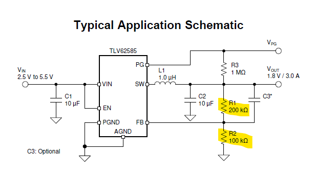
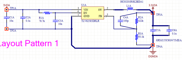
Have a nice day. Recently, I am using TLV62585 the circuit as below:

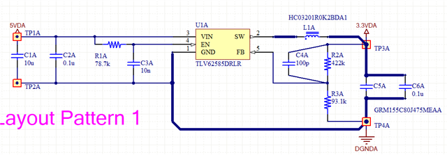
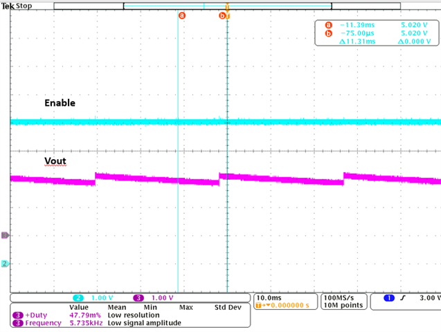
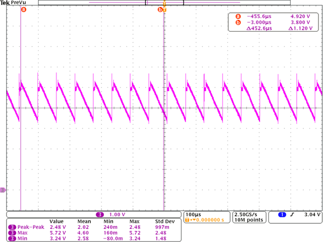
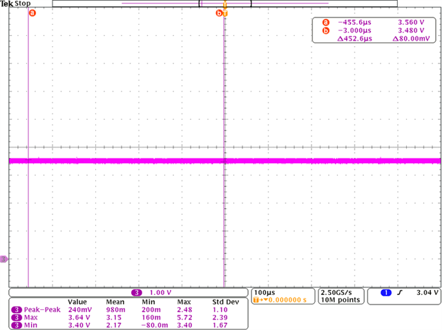
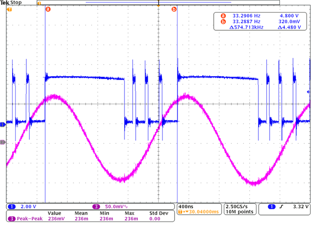
I can't understand why the output waveform is so weird. The output has already changed to 2.2V cause my RfbT & RfbB followed the spec from (432k & 93.1K) change to 

(200k and 100k). 

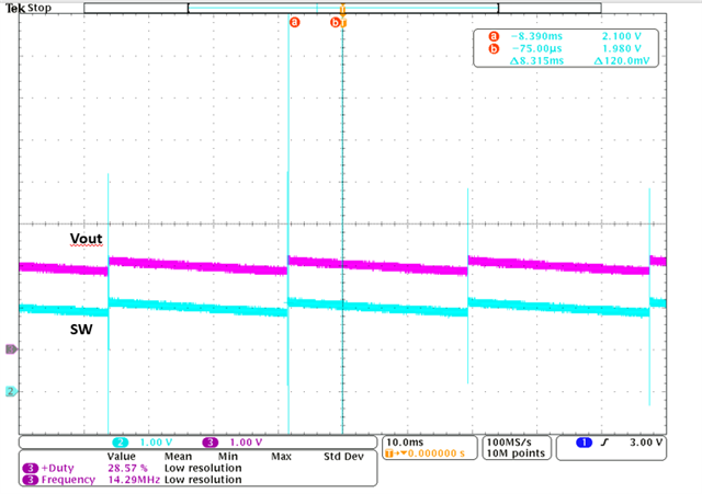
Also, I measured the SW waveform is weird, too. So please help if I misunderstand something.

  • Hello Sway,

    To be able to better understand the issue, could you please clarify the following questions:

    1) I could not find the datasheet of the inductor used in your design. Could you share the datasheet/exact part number of the inductor used in your design?

    2) What did you mean by the following statement? 

    The output has already changed to 2.2V cause my RfbT & RfbB followed the spec from (432k & 93.1K) change to 

    (200k and 100k). 

    Do you mean that you are still getting an output voltage of 2.2Volts? 

    3) Can you also share the waveforms for Vin? 

    4) How are you probing the switch node voltage?  Is the GND connection somewhere near the SW node pin? 

    Thank you!

    Best regards

    Sneha 

  • 1) I could not find the datasheet of the inductor used in your design. Could you share the datasheet/exact part number of the inductor used in your design?

    ans: HC0320-L.pdf @ 1uHhttps://www.atec-group.com/storage/system/product/atwspec/Inductive/Shielded_SMD_Power_Inductor/HC/HC0320-L.pdf 

    2) What did you mean by the following statement? 

    The output has already changed to 2.2V cause my RfbT & RfbB followed the spec from (432k & 93.1K) change to 

    (200k and 100k). 

    Do you mean that you are still getting an output voltage of 2.2Volts? 

    ans: I mean even I change the resistance pair, the ripple voltage is still poor, as the waveform I had posted.

    3) Can you also share the waveforms for Vin? 

    TBD

    4) How are you probing the switch node voltage?  Is the GND connection somewhere near the SW node pin? 

    ans: I use the ok wire to measure it.  It is the same point with Vin & Vout ground. ex: C5A or C1A. When I measure other versions the SW waveform is normal. You can refer to below:

  • Hello Sway,

    Thanks for your reply. 

    The schematic looks fine to me. I do not see any problem with the parameters used in the circuit.

    Could you please share the waveforms for Vout and SW node again with lower time scale ( for ex: 2usec or similar), instead of 10msec ?   

    Also, When you say you are getting normal SW waveforms with "other versions". What does "other versions" mean here? Please let me know.

    Thank you!

    Best regards

    Sneha

  • Hello Sway,

    Sorry I forgot to add this point in my earlier comment.

    It would be great to have Max, Min, frequency values for both waveforms (Vout and SW).

    Thanks!

    Best regards

    Sneha 

  • Hi Sneha,

    I found the C5A may be wrong. It should be 4.7uF, but it placed 0.1uF when sample making. 

    And then I need to some load avoiding the burst mode, so I can see the waveform smoothly.

    However, do you have any recommendations about the output cap, is it possible to be lower? ex: L=1uh, output cap just 2.2uF (C5A) what are the pros and cons?

    Anyway, thanks Sneha kindly support.

  • HI Sway,

    Thanks a lot for the update. 

    We do not recommend using lower capacitor values than datasheet specifications as it can affect the transient performance of the converter. The device is designed to have best performance with the datasheet recommendations only. Unfortunately, we cannot guarantee device behavior outside of datasheet specifications. 

    The following app note explains the input and output capacitor selection procedure:

    https://www.ti.com/lit/an/slta055/slta055.pdf?ts=1648024792643&ref_url=https%253A%252F%252Fwww.google.com%252F

    Therefore, I would recommend to stick to the datasheet parameters. Please also refer to the LC matrix shown in the datasheet in page 10.

    Let me know if you have any further questions. 

    Thank you!

    Best regards

    Sneha 

  • Hi Sneha,

    Do you know how to judge whether the IC is in PSM or PWM? What is the threshold? 0.1A or 3A as the spec figure14 and figure15

    Is it possible to adjust by using an external circuit?

    Thank you!

  • Hello Sway,

    The device enters the PSM when the load current is below a certain threshold value. During the PSM mode, the switching frequency starts decreasing with the decreasing load currents in order to maintain high efficiency.

    So from the switching frequency vs load current characteristics from the datasheet (figure 11), I would estimate the transition point to be around 600 mA.  As you can see that the switching frequency starts decreasing from its typical value as shown in red in the figure below:

    Apart from switching frequency and load current, this transition also depends upon the Vout, Vin, and inductor value. You can find more information on this mode transition in the following app note:  https://www.ti.com/lit/pdf/snva857 

    Thank you!

    Best regards

    Sneha


  • Hi Sneha,

    Here are two more questions that need your help:

    1. Is it 100p too large for C4A, do you have any calculated reference?

    2. Is R3A not recommended to be used below 100k, or is R2A not over 400k?

    CH1: SW node voltage

    CH3: Vo (ac coupling)

  • Hello Sway,

    The feedback resistors and CFF defines the output voltage setting and the transient response of the system. The choice depends upon the user and the application. 

    However, datasheet recommends use a feedback resistor (bottom), R2 lower than 100kohms. Based on this value and the output voltage setting you require, you can calculate the value for feedback resistor (top), R1.

    There are two application notes explaining the calculation for the feedback resistors and feedforward capacitor. I would recommend to have a look into these:

    https://www.ti.com/lit/an/slva477b/slva477b.pdf?ts=1648206729094&ref_url=https%253A%252F%252Fwww.google.com%252F

    and 

    /cfs-file/__key/communityserver-discussions-components-files/196/Design-considerations-for-a-resistive-feedback-divider-in-a-DCDC-converter.pdf

    Thank you!

    Best regards

    Sneha