This thread has been locked.

If you have a related question, please click the "Ask a related question" button in the top right corner. The newly created question will be automatically linked to this question.

BQ24600: Schematic/Design Review

Part Number: BQ24600

Hi TI Team,

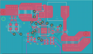
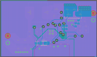
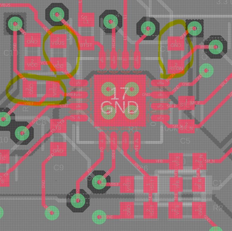
I would like to ask if you could look over my design for the BQ24600, I have followed the datassheet and few examples as my guide when it comes to placing componenets and tracing, I'm just not houndred percent sure about the split of primary ground and analog ground. Please do give me your opinions and suggestions. 

I've used the calculator that you have attached to the page of the device to scale compoenents to fit the specifications.

Specs:

  • Cell Count : 6
  • Vbat : 4.3 V
  • Vbat : 25.8 V

  • Ichg : 2 A

  • NTC selected : ERT-J0EG103JAERT-J0EG103JA 

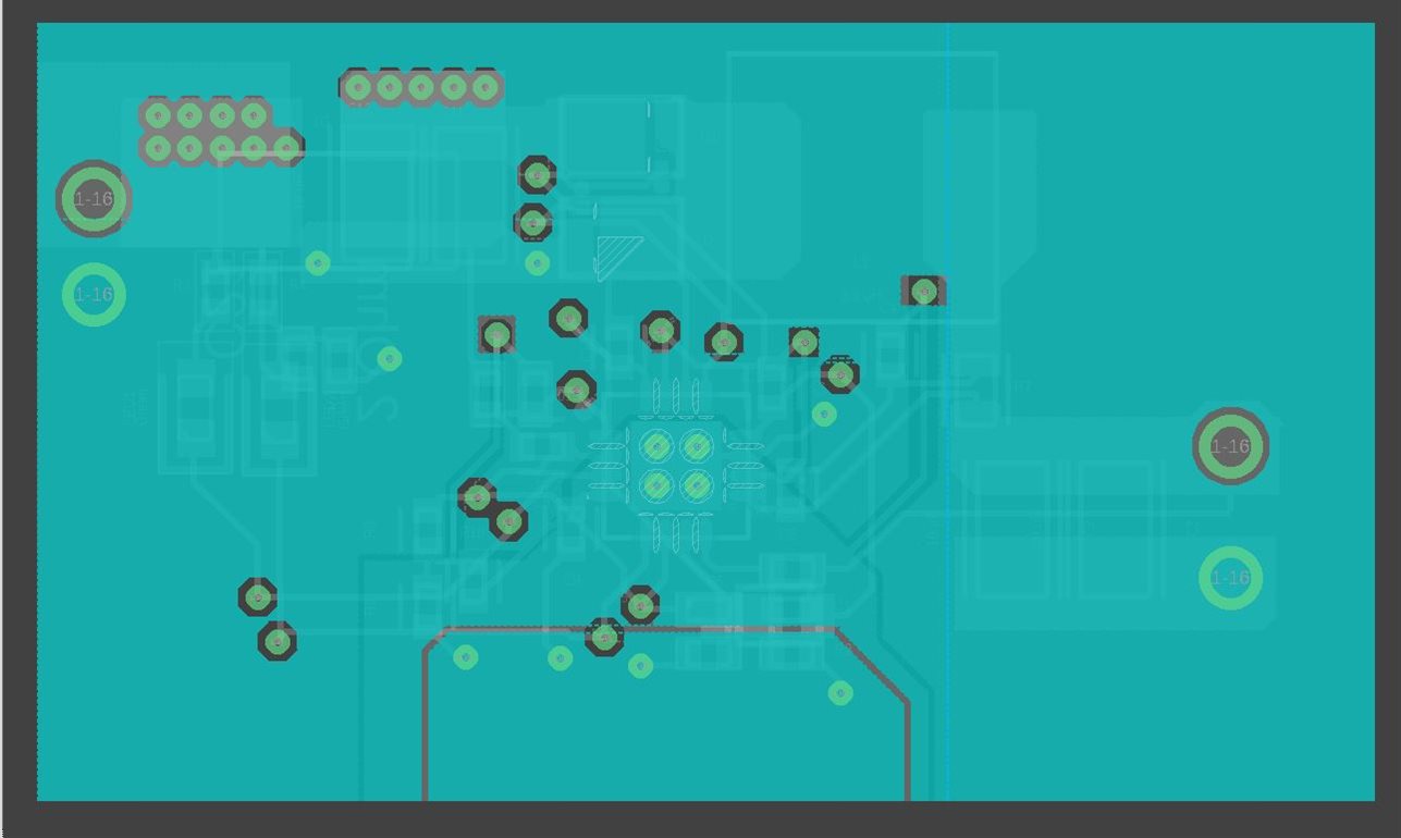
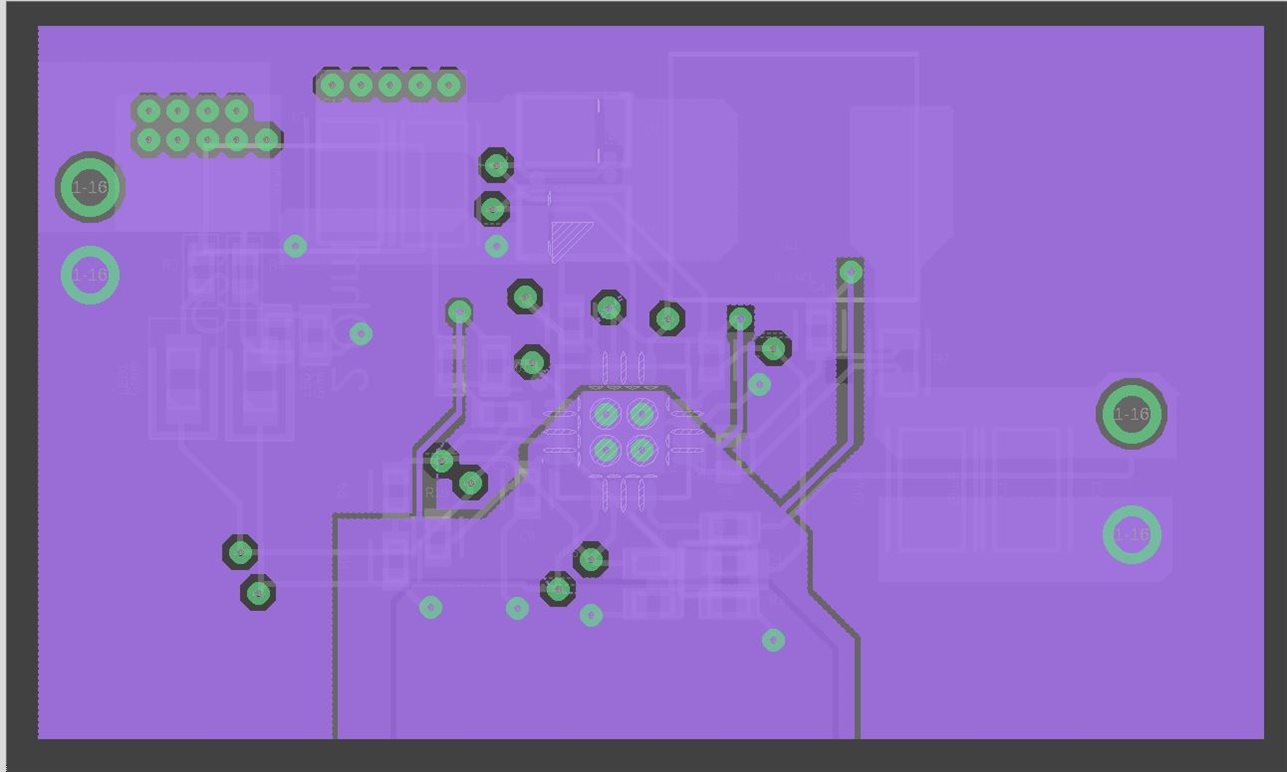
Attached is PDF of the schematic and the top layer outline, as well as a PNG of both top and bottom layer.

3666.Top Layer.pdfCharger Schematic.pdf

  • Hello,

    My schematic review is as follows:

    1. Please change R11 to 2 Ohm for the hot plug filter as shown in Figure 12 of the datasheet.

    2. The charge regulation voltage is 25.2 V.

    3. The charge current regulation is 1.99 A.

    3. Please confirm the thermistor works for your desired temperature range.

    My layout review is as follows (according to the layout guidelines):

    1. The input capacitor is close to the switching FETs.

    2. The switching FET gate drive pins are close to the FETs.

    3. The inductor terminal is very close to the switching FETs.

    4. You could move the charge current sense resistor close to the inductor output.

    5. The output capacitor could be moved closer to the sense resistor.

    7. From the images provided I am having trouble seeing if they are split properly.

    8. Thermal pad soldered to GND correctly.

    9. It does not look like any of your decoupling capacitors for VCC, VREF, and REGN are as close to the IC as they can be. You should not draw current from the pin before the trace reaches the capacitor. In other words, the current should flow from the pin, to the capacitor, and then to wherever it needs to go.

    Regards,

    Mike Emanuel

  • Hi Michael,

    Thank you for your review of my design. I'll follow up on the suggestions that you have given me and correct the decupling capacitors positions. I'll also try to get you a better layer by layer images in PDF format so that the quality doesn't decay. 

    Also I have a question, you mention taht the charge regulation is 25.2V, could you say where I'm loosing the 0.5V?

    Regards,

    Patryk Szczesny.

  • Hi Patryk,

    The equation for charge regulation voltage from the VFB pin is 2.1*(1+Rtop/Rbot) or 2.1*(1+1.1/0.1) = 25.2 V. Please adjust your resistor divider if you want a different regulation voltage.

    Regards,

    Mike Emanuel

  • Hi Mike,

    Sorry for the late response. I have corrected by Rbot with a 97.6K Ohm resistor to get as closer to the regulated votlage. I also had replaced the resistor you have suggested for hot plug filtering.

    As for grounds, please see the attached JPEGs below. Layer 2 (Cyan) is mostly Primary ground with a small section of analog ground that connects analog signal vias from the top layer. The layer 3 (purple) has some analog signals coming from the upper side of the layer where its surrounded by primary ground but isolated from it by a space in copper. On layer 3 the analog ground is also connected to the underbelly of the IC.

    The decupling capacitors have now been moved closer to the IC too like you sugested.

    Kind Regards,

    Patryk Szczesny.

  • Hi Patryk,

    To assist in my review can you please send gerbers files for me to view?

    Regards,

    Mike Emanuel

  • OF course, here's a ZIP file with the gerber files attached. 

    BQ24600 Gerber Files.zip

  • Hello,

    My layout review is as follows from the layout guidelines:

    2. I think the HIDRV gate signal can be routed a shorter distance to the pin on the FET.

    7. As long as the separate grounds are joined at the thermal pad that should be good.

    9. The VCC capacitor is placed farther away from the VCC pin than R12 is. VREF capacitor C8 is not close at all to the VREF pin. Please make sure these decoupling capacitors are the closest component to their pin and are as close as possible to their pin.

    Regards,

    Mike Emanuel

  • Sorry for the late response, thank you for your insight, I appriciate it.

    Kind regards,

    Patryk.