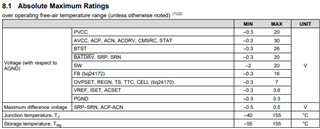
This thread has been locked.

If you have a related question, please click the "Ask a related question" button in the top right corner. The newly created question will be automatically linked to this question.

BQ24172: REGN_pin low impedance

Part Number: BQ24172

Hi  Sir,

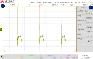
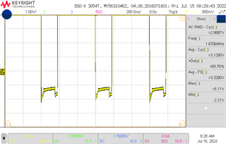
we found that pin_20 REGN seem have low impedance phenomenon,

is there any problem with this schematic? what is the reason for the low impedance od REGN pin?

dp3m_2a_v01z09_BOM_ES1_0a6_5v_adj.pdf

  • Hi Tommy, 

    We'll review the schematic and get back to you by tomorrow. 

    Regards, 

    Arelis Guerrero 

  • Hi Tommy,

    The schematic looks reasonable except for the missing Schottky diode from SW to GND.  That diode is required.  REGN damage can occur from overvoltage at AVCC.  

    Regards,

    Jeff

  • Hi Sir

    Could you explain more about the purpose of this schottky diode?
    The low side MOSFET has body diode should play same role with external schottky diode except the forward voltage drop higher.

    Where is the overvoltage at AVCC come from? From system noise or from internal of IC or from battery inserted?
    We had tried to add a continuous DC 50V to ahead of external input MOSFET and BQ24172 and IC didn't broken.
    What condition will casue AVCC overvoltage?

    Regards,

    Azure

  • Hi Azure,

    The Schottky lowers the losses during body diode conduction, thereby increasing efficiency, and also clamps the SW node from ringing below 0.3V.

    The abs max ratings for the pins is shown below, with AVCC being 30V and PVCC being 20V. So applying 50V most likely damaged the IC.

    Regards,

    Jeff

  • Hi Jeff

    Was the clamping function needed due to minimum value of REGN -0.3V or -2V SW pin?
    I can't find any spec reagarding this diode in datasheet.
    Schottky diode should share the current while switching MOS dead-time only.
    Can I select 40V 1A SOD123 schottky diode? Like Diodes 1N5819HW-7-F
    Could you sugesst part no. for this diode?

    Regards,

    Azure

  • Hi Jeff

    Updated SW pin waveform with and without Schottky diode.

    The undervoltage level from -4.25V to -4.0V with diode.

    Could you judge the noise was good enough or not?

    Regards,

    Azure

    0714_SWpin-wD_0a1.pdf

  • Hi Azure,

    The schottky diode only turns on during IC high side FET dead time.  The EVM uses 2A B220A-13-F  from Diodes Inc.  

    Regarding the undervoltage measurement on SW pin, -4V seems a bit much.  Are you measuring with a short ground link shown below?

    Improved PCB layout, especially, the capacitors from PVCC to IC GND will reduce this undershoot.

    Regards,
    Jeff

  • Hi Jeff
    Using short wires to ground, the UV of SW node became -2.2V with diode and -2.9V without diode.
    SW node without diode  SW node with diode

    There was about 10 pcs BQ24172 IC couldn't charge battery on board after shipping by air.
    Before replace IC, check SW pin and no 12V level.
    the chip seems no open/short after TI I/V curve on REGN pin.
    However, the failure unit I/V curve didn't trace the good unit.
    Refer attached pdf file in detail.

    QEM-CCR-2207-00202 Final Report(unit 2).pdf
    Could I clarify sereral points below again?
    Would no diode at SW cause the SW node had UV?
    Would the UV at SW node cause the AVCC over voltage?
    Would the AVCC over voltage cause REGN node abnormal?
    Would the diode be root cause and make charge IC couldn't charge battery?

    Regards,
    Azure

  • Hi Azure,

    I would not expect the missing diode on SW to cause damage or prevent charge but I have very little data for this device without the diode.

    I do not expect UV on SW to cause AVCC damage.  

    I do expect OV on AVCC to cause REGN damage.

    Regards,

    Jeff

  • Hi Jeff

    Do you have any idea reagarding the REGN lead leadage current of failure unit in the report?
    IC didn't have open /short but they didn't work on board.
    We got the I/V curves report for AVCC, PVCC, ACP, SRN, VREF, REGN, BTST, SW.
    There was REGN node I/V failure only.
    Where did the big energy come from input (AVCC), output (battery) or chip switching noise?

    Regards,

    Azure

  • Azure,

    I do not have any more data for this. Is it possible that the PCB had a solder short or that one of the capacitors on AVCC or REGN failed as a short?

    Regards,

    Jeff