- Ask a related questionWhat is a related question?A related question is a question created from another question. When the related question is created, it will be automatically linked to the original question.
Hello TI Team,
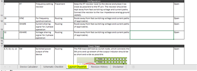
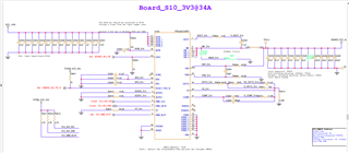
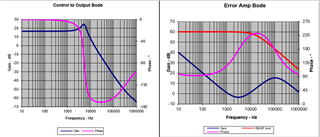
We have done the schematic design of TPS546C23 buck- regulator with help Design Excel sheet calculator. Kindly review the Schematics, Bode Plot and thermal point view and share your valuable feedback.
Requirements:-
Design 1. 1.3V@10-13A , O/P ripple= 10mVp-p, Voltage tolerance= 1%, Vin=12Vdc, FSW=300KHz
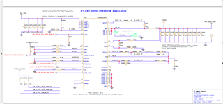
Design 2. 3.3V@30-34A, O/P ripple= 9mVp-p, Voltage tolerance= 5%, Vin=12Vdc, FSW=300KHz
Design 3. 0.88V@16-20A, O/P ripple= 20mVp-p, Voltage tolerance= 3%, Vin=12Vdc, FSW=300KHz
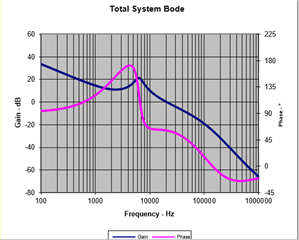
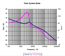
We have attached bode plot from design calculator Please review Bode Plot (for Compensation circuit confirmation)
Design 2:- 3.3V@30-34A, O/P ripple= 9mVp-p, Voltage tolerance= 5%, Vin=12Vdc, FSW=300KHz
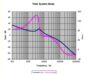
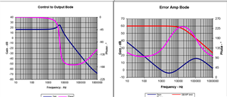
Phase Margin=61.4Deg.@20.2KHz cross over frequency
Gain Margin=-23dB
IC Power Dissipation:- 4.069W(As per calculation TJ going Out of recommendation)
-------------------------------------------------------------------------------------------------------------------------------------------------------------------------------------------------------------------------------------------------------------------------------------
Design 1:- 1.3V@10-13A , O/P ripple= 10mVp-p, Voltage tolerance= 1%, Vin=12Vdc, FSW=300KHz
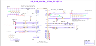
Phase Margin=61Deg.@20.5KHz cross over frequency
Gain Margin=-25.3dB
IC Power Dissipation:- 3.265W(As per calculation TJ going Out of recommendation)
---------------------------------------------------------------------------------------------------------------------------------------------------------------------------------------------------------------------------------------------------------------------------------
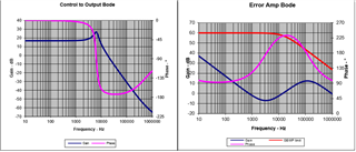
Design 3:- 0.88V@16-20A, O/P ripple= 20mVp-p, Voltage tolerance= 3%, Vin=12Vdc, FSW=300KHz
Phase Margin=60.5Deg.@22KHz cross over frequency
Gain Margin=-25.9dB
IC Power Dissipation:- 2.7W(As per calculation TJ going Out of recommendation)
Please help here in reviewing and share your comments.
Thanks & Regards,
Prasad Tatar