This thread has been locked.

If you have a related question, please click the "Ask a related question" button in the top right corner. The newly created question will be automatically linked to this question.

LP87561-Q1: LP875650RNFTQ1 design

Part Number: LP87561-Q1

Hi, 

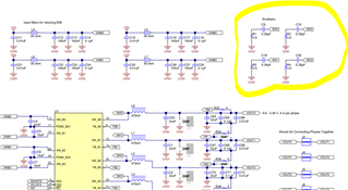
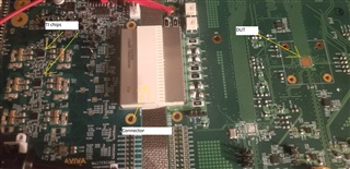
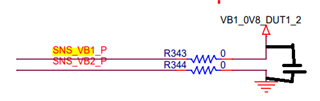
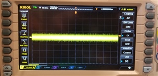
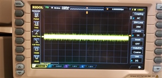
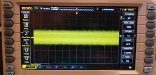
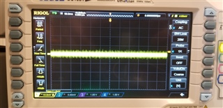
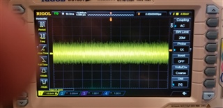
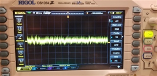
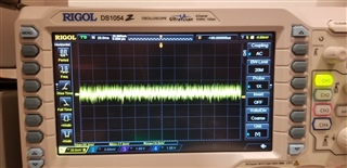
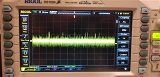
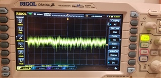
schematics is attached.  the design is done, and the board is in the lab.  The voltage come out properly and the current and voltages can be read.  however, i am not trusting the current reading.  the main issue is that the chip gets hot under no load condition.  Does not matter if you have any load on the power supply, the chip gets so hot that you cannot touch it.  under no load, I am noticing that the chip draws about 1.5A.  Please review the design and let me know how to resolve the issue...

thanks,TI_Review_09232022.pdf

Habib

  • Hi Habib,

    Snubber capacitors in the schematic are 1000 times larger than the recommended. Recommended snubber cap is 390 pF.

    Also, the feedback connections are a bit odd. What are SNS_VB1_P, SNS_VB2_P, SNS_VB3_P and SNS_VB4_P sensing? Are there two feedback paths since there are also some 100 Ohm resistors populated?

    FB0 should be connected to the point of load of 0.8V rail. FB1 should be connected to GND of the 0.8V and routed differentially from the point of load. Similarly for FB2 and FB3, FB2 senses the voltage and FB3 senses the GND of the 1.25V rail.

    BR,

    Samuli

  • Hi Samuli,

    thanks for your quick response, your suggestion resolved the heating issue.  but i still see some another issue with my design.  before explaining that issue, please note that the snubber values were taken from your evaluation board design which i have pasted a picture of it at the end of my email....

    you had a question about the sensing; 100 ohms are used to sense locally, and zero ohm is used to sense close the DUT card.  Sometimes the DUT is not available and i don't want to leave this FB point not connected to anything.  but when the DUT connects, 0ohms overtake 100 ohms to sense the DUT card.  please let me know if this method will cause any issue...

    the other issue that i have is that i have connected electronic load to the output of a 2 PHASE and it shuts down the power beyond 2A.  please let me know if i am limiting the current in the design or there is something else wrong with it.  i am assuming each phase is capable of 4A..

    thanks,

    Habib

  • Hi Habib,

    It seems that there is a mistake in the Altium design file schematics with the snubber capacitor size but they are correct in the EVM user's guide schematics. My apologies about that.

    The feedback connections could be the cause of the issue shutdown issue. A regulator will shut down on short, thermal protection, input over voltage or undervoltage as well as EN and NRST signals. Seeing scope shots from the input and output voltages when the device shuts down would be really helpful.

    BR,

    Samuli

  • Thank Samuli for the quick response.

    ok, I understand what your approach is to resolve this issue, yes, feedback connection could be the cause of this issue as well.  also, that there is connector on the feedback path that might add inductance to the line and cause some issue. I will do more experiment and will give you your requested plots to resolve this as could as possible.

    thanks,

    Habib

  • Hi Samuli,

    Just a quick update is that if i put the load on the DUT card as i have labeled on the picture below on the right side of the connector, i can only increase the load to 2A before the TI switcher shuts down.  however, if i put the load close to TI switchers which is on the left-hand side of the connector, i can increase the load to 8A.  that is why i think the connector is messing with the feedback line.  please let me know how to proceed.  because i would like to be able to sense the feedback on the DUT card close to the chip to compensate for the plane drop.

    thanks,

    Habib

  • Hi Habib, 

    Thanks for reaching out! Our customer support team is unavailable Monday and Tuesday October 17-18th due to all-day workshops. Please expect a delayed response. Thank you for your patience. 

    Regards,

    Garrett

  • Hi Habib,

    Does the regulator work with the connector if the 100 ohm resistors are not populated? Having a long feedback loop will add significant inductance into the loop and could cause instability. This could be verified by probing the switch node. The instability may be countered by adding additional capacitance. 

    See the below application note for some measured stability numbers on the EVM.

    www.ti.com/.../snva881

    BR,

    Samuli

  • Hi Samuli,

    removing the 100 OHMs did not help.  where should i be adding the capacitance to stabilize it? on the feedback line in parallel to 100 OHMs?   i will take some photos of switching bodes too. please suggest some capacitor value to try to see i can improve the load...

    thanks,

    Habib 

  • Hi Habib,

    The capacitors should be at the point of load. In other words, at the point where the feedback is sensed from. In this case it would be close to the DUT on the board.

    BR,

    Samuli

  • So, assuming below is my sense lines.... i should have a connectivity like what i am showing below?  by the way the reason these both lines are called _P on both ends is that this design is implemented to cover all the phases, right now we are using 2+2 phase..

    thanks,

    Habib

  • Hi Habib,

    The capacitor should not be placed between the feedback traces but it should be connected between the VB1_0V8_DUT1_2 and GND planes close to the load. Strong connection to both nets. How much capacitance does the DUT board have on VB1_0V8_DUT1_2 net?

    BR,

    Samuli

  • Hi Samuli,

    Thanks for all your quick responses and thanks for being right spot on the point.  Your suggestion worked and I increased the capacitance on the DUT card from 22uF to 44uF and seems that I can pump in more current.  I will leave a great review for your help.  I still need your help for one more thing.  I have pasted the pictures of my ripple measurements under different load settings which were achieve by an electronic load.  I would like to decrease the ripple on low load condition such 100mA to to around 20mA from 30mA reported below in the picture.  I also see that the regulator has higher ripple under 6A load compare to 7A load.  please review the pictures below and let me know if they make sense to you.  but my most concern is to reduce the ripple under low load since our single chip draws about 50mA on 2 rails... the picture names define the load conditions...

    thanks,

    Habib

  • Hi Habib,

    In low load conditions the device switches in PFM mode which improves efficiency but creates more output voltage ripple. If the low load efficiency is not a concern for you then you can write BUCKx_FPWM to 0 to improve the output voltage ripple. BUCKs could also be forced to work in multiphase mode by setting BUCKx_FPWM_MP to 1.

    Register setting can be found for BUCK01 in address 0x2 and for BUCK23 in address 0x6.

    Below is a transition from PWM to PFM.

    BR,

    Samuli

  • Hi Samuli,

    Thanks for your response, we do care about the low load efficiency since we are measuring the current at low load around 50mA for some rails.  so, if i change it to PWM mode, we might not be reading the correct current numbers.  is this a correct statement?  

    also, please suggest a reason for 6A increased ripple, i need to know why it is increased to high 20mA range ripple... other than that, I think I should be done with my characterization. 

    thanks,

    Habib

  • Hi Habib,

    PWM mode keeps the switching frequency constant and you will still get correct current reading. Output voltage and current ripple will be less in PWM mode but efficiency will also be worse. You can verify if the PMIC is switching in PFM or PWM mode by probing the switch node of the buck.

    Hard to say about the 6A ripple increase without seeing the switch node. It could be that the regulator is close to being unstable in that region or it is because the duty cycle reaches 50% which is the worst case for the current ripple.

    BR,

    Samuli

  • Hi Samuli,

    i am seeing one more issue, i have configured this TI chip into 2+2 phase design.  all we have been analyzing so far was the first 2 phases which the output is set to 0.85V.  however, on the second phase, which is combination of VB3+VB4, the output is set to 1.25V.. i see the level of noise is too much under any load. my question is that is there any change in the chip setting that i am doing wrong since the outputs are different?    0601.TI_Review_09232022.pdf  please see my measurements below.. i also resending the schematics again.  please note that i am measuring the combined output of VB3+VB4...

  • Hi Habib,

    Probably same issue with this rail as well as with the other one. There is not enough point of load capacitance at the feedback sensing point. Since the power plane and feedback go through a connector there will be significant inductance in the loop which may result in instability. I would recommend adding point of load capacitance to this rail on the DUT board as well.

    The TI recommendation is to have 22 µF local capacitance for each phase, in your case that is on the main board with the PMICs. Then have 22 µF at the point of load close to the DUT for each phase. Since the power plane and feedback go across the connector I would recommend 2x22 µF/phase (4x22 µF for 1.25V and 4x22 µF for 0.85V) on the DUT board. The other option is to take the feedback from the main board that has the PMICs.

    BR,

    Samuli