This thread has been locked.

If you have a related question, please click the "Ask a related question" button in the top right corner. The newly created question will be automatically linked to this question.

LMG3411R150: LMG3411R150 isolator issues

Part Number: LMG3411R150
Other Parts Discussed in Thread: ISO7831, UCC27712, LM1117, LM3410

Hi TIer,

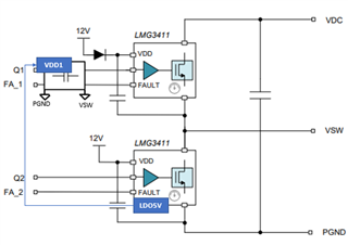
We plan use LMG3411R150 design for totem pole PFC high speed leg in daughter card.

In 4 layer PCB and only use TOP layer to placement, and bottom just use to cooling with housing. found out the best isolator solution is Infineon's SOI Level shift such. because there is no iso-power need.

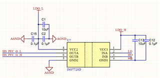
if use iso-power with digital isolator such as SN6506 with ISO7831, consider the good layout, need use top and bottom layer.

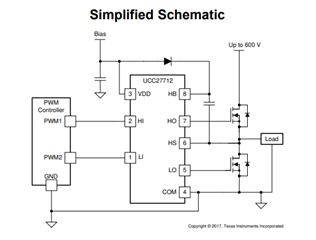
so, may I know TI have half bridge level 600V shift solution?

  • Hello,

    On the EVM for this device we use the SN6505 as the bias supply controller and the ISO7831 as the digital isolator. I need some time to give you the best answer on TI's level shifters. I'll make sure to get you a response by the end of this week. 

    Best Regards,

    Kyle Wolf

  • Hello, 

    You can use TI's UCC27712 620V high-side low-side gate driver. When using this device with our GaN devices you will want to use the bootstrap diode to supply voltage to the HB pin of the UCC27712 as well as the VDD pin of the GaN device. You will also want to place a capacitor between HB and HS close to the GaN device as well. Also the absolute max. voltage of the GaN device's IN pin in the data sheet is 5.5V, to account for the difference in output voltage of the UCC27712 and max. input voltage of the GaN device you can use a voltage divider between HO and IN and IN and HS. 

    Please reply with any questions or for more clarification.

    Thank you,

    Kyle Wolf

  • Dear Sir,

    thank you very much! May I  know if the 50V/ns dv/dt immunity of the UCC27712 is affected by the GAN switching

  • Hello,

    The LMG3522R150 has an adjustable slew rate feature. The slew rate can be adjusted from 25 V/ns to 100 V/ns, if you would like to use the UCC27712 the slew rate selected would have to be below the 50V/ns dv/dt immunity level. If your system requires a slew rate above that a different gate driver would have to be selected. Please reply if the system requires a different gate driver to be selected and I can help connect you to the right person.

    Thank you,

    Kyle Wolf

  • Dear Sir,

    thank you very much! looks the UCC2771x series are not pure for Driver GaN use, and I think efficiency affected by low turn on slew rate.  

    I found the NCP51820 which has 200V/ns immunity capability from onsemi web.

    May I know if TI has a higher dv/dt immunity half bridge IC can suggestion? thanks again.

  • Dear Sir,

    also need you help me to review the following concept.

    ISO7431 powered form low side LDO5V of LMG341x.

  • Hello,

    I am answering on Kyle's behalf, but I have been following this thread and consulted Kyle about the issue.

    The concept you shared would work in theory, but may not be the best approach depending on your setup. In situations like this, usually the supply voltage for the isolator can be borrowed from whatever controller is used for the input signal. That way the high an low side stay as separated as possible. I do not know what your input setup is, and as I mentioned the concept you shared would work in theory, just wanted to give you some more background information.

    For your gate driver question posted earlier, I will add our gate driver team to this thread so they may provide you with more technical assistance.

    Regards,

    Zach

  • lmg3410 with iso7721_LDO version.pdf

    lmg3410 with UCC27712.pdf

    Dear Zach, Kyle,

    Thank you very much! I'am draw schematic for above two concept for discussion.

    please help us to review it. if have anything errors or any miss, please inform me.

  • Hello,

    First I will discuss the gate driver schematic: The VDD pin of the gate driver (UCC27712) should be connected to 15V not LDO_L. Also, the outputs from the gate driver (HO and LO) will be referenced to the HB and HS voltages, meaning they will sit at ~15 V when high. The input pins for the GaN fets should sit at 5 V max when high, so you will need to add a voltage divider to step down your input pin voltage. If you need more clarification on this let me know.

    For more information on UCC27712, I encourage you to look at the datasheet, here is a simplified schematic to reference:

    Next for the isolator schematic: I do not understand why you have an LDO (LM1117MPX) in your schematic. The LDO5V pins on the GaN fets are outputs, and therefore are used to power other components like isolators, they themselves do not need power. Additionally, the signal "HS PFC G H" should be connected to pin 3 of the isolator not pin 2. Or you could move the signal on pin 6 to pin 7 instead, doesn't matter. Let me know if you need more clarification on this as well.

    Regards,

    Zach

  • Dear Zach,

    thanks for your advise.  

    for gate driver schematic, we not adopt the concept, since the voltage divider may cause the slew rate issues.

    for isolator schematic, the question 1 will swap the pin and question 2 the LDO5V of LM3410 and LM1117 is alternative to VCC1 of digital isolator.

    Do you have better suggestion, please advise.

  • Hello,

    Thank you for the clarification. Are you worried that the LDO5V from the GaN FET will not have enough power to supply the isolator?

    If you do plan to use the LDO however, make sure to adjust the net names appropriately. The "LDO_L" net name should not be used for both the GaN FET and LDO and Isolator.

  • thank you sir.

    a last question is the ISO7720D whether can reverse direction as following figure?

  • Hello,

    Your figure has some problems, allow me to explain:

    The reason we use an isolator for signals to the half bridge is to account for the different reference potentials between the high side (Vbus to switch node) and the low side (switch node to GND). Therefore, the input/output voltages for the high side device need to be level shifted up when compared to the low side.

    Because of this, a single isolator cannot connect to both FETs, the voltage references are different so two isolators need to be used. If the control circuit is referenced to the same GND as the low side, then no isolator is needed for the low side device so just the high side isolator is required.

    So to summarize, your HO and LO signals cannot be used in the same isolator, they must be split up.

    Regards,

    Zach