This thread has been locked.

If you have a related question, please click the "Ask a related question" button in the top right corner. The newly created question will be automatically linked to this question.

UCC28782EVM-030: Values of RTZ AND RDM with load

Part Number: UCC28782EVM-030
Other Parts Discussed in Thread: ATL432, UCC28782, TL431

Hello:

Pl see attached ppt copied from the EVAL kit document.

The table shows how Rdm & Rtz change with load.

How does one interpret the Table?

It is clear that a design is calculated with nominal input & some specific output voltage( min max load) as evidenced by the Spreadsheet Calculator.

A module if built upon these values. Tets are conducted to note vaious characterisrics of the module: expected to satisfy requirements at all "4 corners" as noted in the file.

After this, there is no scope of changing Rdm, Rtz or for that matter ANY value: turns ratio, Rcs, etc..in a delivered functional module...

Does the Table imply that for input/output variations, a fixed design IS NOT OPTIMAL?

Or does it imply that for different input/output ranges, values will be different?.. which is clearly self-evident?

In this latter case, should one not depend upon the results of calculations from the Spreadsheet?

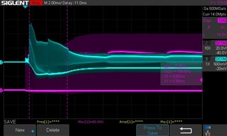
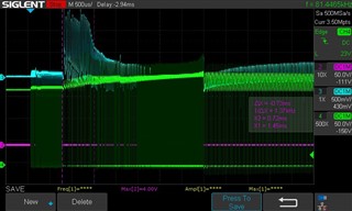
Our search is to find which values of Rdm, Rtz, Rvs1, Rvs2, Rcs, Rsws, Csw  and Ropp will not cause failures due to mode transitions as load changes, or during transitions to/from ZVS.

Our design is all GaN based. All components are close to 1% TOL, so the only variants are Vin and Load.

Appreciate any light you can throw on this issue of "optimization" that would have inherent stability in this wider sense to a design.

-r

load_vs_values.pptx

  • Hello Robin,  

    In the table, Rdm and Rtz appear to change with load, but they do so because the parameters in their equations change in such ways that also are affected by load. 

    Rdm is intended to "tell" the controller what the demag down slope will be and is a function of Lm, Nap, the VS divider ratio, 1/Rcs, and a constant.  One designed, none of these factors will change regardless of input or output conditions. Rdm is based on nominal values so that the down-slope is always "down the middle" and the ZVS tuner function has ample room to accommodate reasonably-wide tolerance variations and still be able to adjust the necessary negative current on-time for PWMH.

    Rtz is intended to "tell" the controller when to turn on PWML after a calculated delay time from the falling edge of PWMH.  In this case it is a function of Vbulk, Vout, Lm, Cswn, Nps, tD(dr), and a constant, but this time not all of the factors stay constant.  The design target is at the Vbulk(max) for minimum LC ring timing and the controller automatically expands the timing at low-line conditions.  Here, however, Lm can vary part-to-part and the true Cswn is highly non-linear.  However, we try to estimate an equivalent lumped element value for it for calculation purposes.  If Lm, Cswn, and Nps all vary with power level, then certainly Rtz will also vary.

    It is true that once the values are fixed, there is virtually no chance for variable optimization.  Rdm really shouldn't change from the calculation, but Rtz can be adjusted up or down while evaluating a prototype board to find its optimal set point.  Since it depends on a Cswn estimation, if that estimation is off, timing performance may not be optimal, but can easily be adjusted once a board is running.  You have to have something there to get the first board running; then you examine Vds for ZVS and adjust Rtz as needed, if needed. 

    A similar discussion can be made for the other resistors and capacitors in the table.  They are all calculated from nominal component values and estimated parasitics, actual variations may deviate enough to make the performance sub optimal over a wide range of conditions.  So each function can be adjusted based on waveforms gathered during evaluation, and values tweaked to improve performance in a certain direction. 

    Note that, with fixed components, it is not possible to have optimal performance at each and every operating condition, so the optimal point should be chosen at the conditions where it is most important to be optimal (what ever attribute is defined for optimality), such that all other conditions demonstrate gradually less optimality as the conditions move away from the optimal point. 
    I definitely do recommend using the Calculator tool to generate the values for your design.  Then evaluate that design and adjust where it seems necessary to adjust. If the adjustment doesn't bring about an improvement, then revert back to the starting point. 

    The values of Rdm, Rtz, Rvs1, Rvs2, Rcs, Rsws, Cswn and Ropp have nothing to do with causing failures due to mode transitions as load changes, or during transitions to/from ZVS.  Failures during mode transitions are caused by electrical overstress, usually from unclamped voltage spikes from excess stored energy somewhere.  Sometimes other events. The mode transitions are going to happen at some operating points, regardless of what those resistor values are.  A cautious bring-up of the prototype board will allow identification of any potential overstress while it is still sustainable and steps may be taken to remedy it, if not already predesigned in.   

    Remember that the main point of the ACF topology is to achieve the highest conversion efficiency by utilizing the same parasitic elements that normally cause high losses as a means to recapture and deliver that energy to the output.  But we're trying to do that with semiconductor parasitics that are loosely "controlled" and change their value significantly with conditions.  The optimal operating component values are not all likely to be the values calculated from the Excel tool, but they're the best place to start. 

    Regards,
    Ulrich

  • Hello Ulrich:

    Once again, grateful for your detailed explanation of the design setup.

    Fully agree with your POVs.

    Indeed, I suspect there is SOME OTHER transient on Vds or Vgs in our GaN SR( EPC2034). We blew once more yesterday at 1 amp load!

    The module was shutting down at around 2amp. Working with HP 6060B E/load. Trusting its characteristics.

    It is possible long ( <2" ) secondary transformer service loop is one contributing factor.

    I suspect std probes are not catching these transients. 

    "A" sold "divide by 10" or the Siglent digital scope may not be showing them either....going to use a Tek scope now.

    Setting up with HP 41800A Active HF probe (with an attenuator)... hope to find these & add "Spike killers" where needed.

    Will keep you posted on this.

    -r

  • Hello Ulrich:

    We suspected something amiss in the design or values...Pl see attached I(Rcs) vs  PWML. I suspect the negative part of I(Rcs) is the root cause of the problem. We are still looking for its source. It is the same assembly that was our work-horse until it wasn't. But having blown last GaN, we added a SiC beast at the secondary rectifier circuit...for now, until we fix the primary side.

    Any idea where this negative part of I(Rcs) coming from?

    -r

  • Hello Robin, 

    Thank you for the screenshot of V(Rcs) and Vds (it's not PWML).  These waveforms are "semi-normal" in the sense that they can be explained and are expected under certain circumstances, but contain aspects that are not quite right for the operating conditions.  

    To be more explicit, the negative current part of the Rcs voltage waveform is normal and appropriate for a high-line condition, but seems excessively negative for the low-line case.  From the drain ringing (apparently after a burst) I estimate that AC input is about 120Vrms, and that the reflected voltage is about 60V.  
    With the bulk voltage around ~160Vdc, the reflected demag voltage should naturally ring down to ~120V, but some Ineg built up after each demag time will force Vds to achieve ZVS.  The mechanism and waveforms are normal.  My concern is that there seems to be too much negative current and that Vds is being driven to ZVS too forcefully.  We see Vds being kind of "hammered" below GND rather than gently rolling to GND. 
    So we have to figure out why PWMH is apparently staying on longer than necessary to build up more Ineg than necessary to get ZVS.

    A second concern of mine is the last pulse Vds waveshape after the demag.  Assuming that this is the last pulse of an ABM burst, PWMH is suppressed and I would expect the reflected voltage to roll off and ring down from the peak level with an LC characteristic.  Instead, we see a sharp drop as if it is being forced down with some Ineg, but not enough Ineg to force it all the way to GND.  Once that Ineg is used up, it returns to the usual DCM ringing. 

    Maybe this is indicative of a "leaky" high-side MOSFET that stays on too long or somehow allows some Ineg to build up even after PWMH has gone low or isn't even there.  That may explain why there is too much Ineg for the middle burst pulses, and some unwanted Ineg at the last pulse.   

    Please check your high-side gate drive to ensure that it is decisively turning off the high-side FET when PWMH goes low and reliably keeping it off when there is no PWMH.  Also verify that there is no sneak path around the high-side FET that could allow some unwanted Ineg to build up.  
       

    Regards,
    Ulrich

  • Hello Ulrich:

    Never will get tired of typing : thank you for your review & comments!

    Indeed, the upper GaN switch or the ISO731-F - either looked very suspicious. Changed the Isolator, it only got worse!

    Maybe we have beaten up this assembly way beyond recognition( old military affectionate appellation used to be FUBAR).

    Our objective is to find the root cause of EPC2024 popping- and it is good enough to work with a SiC diode that is a beast that will not break in any situation.

    Going to move on to another assy & dig.

    Will post when results look confounding or inspirational...LOL

    r

  • Hello Robin, 

    One other thing occurred to me to recommend for you to check: 

    If you are running a USB-PD charger at 20V (or some voltage higher than 5V) and unplug the load from the PD cable, most USB controllers will default to 5V operation, shut off PD switch and bleed down the output to 5V.  But this leaves high voltage on the clamp cap.  If one plugs in a load that forces the converter to put out full power, PWMH will drive the high-side FET (GaN or Si) and the first pulse that turns on that FET will discharge the stored high voltage charge into the output.   The voltage difference (reflected) will determine a peak current through the LC impedance based on Lleak/Cclamp.  

    We have seen that this peak current can be very high, so either the SR Fet and high-side Fet must be large enough to withstand the highest peak, or what we did was to program the USB controller to reduce the internal voltage from 20V to 5V in small steps to keep the peak currents small within the ratings of the FETs, before turnign the USB switch back on.  

    Please check if your USB controller can do that.

    Regards,Ulrich

  • Ulrich:

    A very timely question you raise: I have started to think if we are not testing the module with wrong load behavior.

    #1: note that we do not have any USB load per se. Not even the WT6636. Our output right now is simply electronic load. Which can be set as cc-mode or CR mode.

    #2 Related question is: can the controller be treated as if it was designed to behave like a typical "power converter" with low output impedance through voltage feedback ( ATL432) ?...since the output voltage regulation is very good when it works, I presumed, indeed it can work like a typical AC-DC converter.

    And that it becomes a USB PD only when the WT6636 type of secondary controller is hooked up.

    #3 True characteristics of a "charger" should be to see a battery as a load; the battery could be in total discharge mode( 0V, right?), even then the controller should be able to keep its maximum constant current output driving into a 0V at t=0, will remain so until the battery gets to a certain pre-assigned voltage level when WT6636 algorithm starts to cut back charging current. 

    But so far, we have strictly tested the assembly as if it was an ac-dc converter. Is that the correct way of testing?

    Your point about the USB connection will be very helpful to remember as we progress to test it as a charger with WT6636 board attached.

    In our development scheme, we made a "front end rectifier" as a module you attach to it if so desired. We have a separate assembly with WT6636 & USB connector we will attach later when we get our basic module to work up to 100W

    So it is quite clear we assume UCC28782 as designed can be used as a board-level "DC-DC" converter if the customer applcaiton is for dc-dc . I that correct way of thinking about its inherent voltage feedback nature?

  • Hello Robin, 

    For Q#1:  You should be able to use your e-load in either CC or CR modes with the ACF converter.

    For Q#2:  Yes, this is a "typical power converter" as you imagine it, and should work like any typical AC-DC converter. 

    For Q#3:  Not quite.  No good battery (of any chemistry) will ever be fully discharged sitting at 0V.  If it is 0V, the battery is very dead and cannot be recharged or brought back to life.  A good fully-discharged battery will still have some open-circuit voltage still somewhere near its fully charged level.   
    Connecting a bad battery to a charger( even with the appropriate charge controller) might lead to overheating of the battery.  

    Furthermore, if the battery voltage stayed near 0V while the converter was trying to charge it, it would operate in OPP for some duration (max time limited to 160ms) but may shut down sooner because the low Vout (clamped by the battery) wouldn't be high enough to reflect to the AUX winding and sustain VDD. 
    If the VDD boost circuit is implemented, it may overcome this problem provided that sufficiency energy can be delivered to the AUX winding that isn't drained off by the depleted battery load. But then you'll still hit the 160ms OPP time limit. 

    A USB or downstream battery charge controller should limit Iout to a maximum level which a normal battery can tolerate and the design OPP threshold should be above that level.

    Later on, your basic DC-DC converter should work okay with a front-end rectifier module, and a back-end USB module where the USB controller takes over control of the voltage feedback loop.   

    Regards,
    Ulrich

  • Thans Ulrich!

    We are going to dig more deeply into the waveforms. We know there is no surge current in this topology with its unique controller- measured output rise & start up current a while ago,

    One thing we will do now is to dig into Vgs and Vds. GaN has some constraints on these. EG : Vgs must be >5 but less than 5.2v...ringing inclusive.

    Syartup drain cannot go beyod 2V in which case EPC draws exccessive current>> high dissipation.

    Meanwhile, THANKING YOU FOR THE SUPERB HELP  THROUGHOUT 2022.

    Happy Holidays & Merry X'mass.

    Safe trip ..if you are traveling...

    -r

  • Happy New Year Ulrich.

    I think we have isolated the root cause of SR device- be it HSON MOSFET or GaN- the reason is the startup current through the SR.

    Pl see attached jpg scope pictures. 

    The interesting thing is it is never mentioned in any document I have tried to read on the topic- although it is as old as flyback topology & all failures in diodes I have come across even in Aerospace applications. This failure type many times burnt up the output tantalum capacitor(s) as well.

    Since it is the output capacitor charging state that causes it, we have mitigation possible- of course adding something in the capacitor return path. Hopefully,  ss ripple will not get worse with our fix. It only helps reduce the duration of the peak set of current pulses through the output SR.

    Before we go ahead, I thought getting your comments on the root cause. There is nothing else that could cause SR failure.

    Any reviews will be highly appreciated.

    r

    Original peak duration: like 5.6ms, peak approx 15 amp

    After the fix: like .55ms,maybe 13 amps

  • Hello Robin, 

    That certainly is an interesting observation.  Definitely, a discharged output capacitor will demand maximum current from the power stage until Vout approaches regulation.   

    I'm thinking that maybe an old-fashioned soft-start circuit on the TL431 can mitigate this, by keeping the initial opto-coupler current high and gradually reducing it for more power.  The down-side is that it will increase start-up time.   
    Maybe there is a compromise point where the soft-start is pretty fast, but slow enough to keep the peak currents within the capability of the SR Fet. 

    After soft-start is complete, it gets out of the way and have no further effect on output ripple or transient response.

    Although it is easy enough to add to a TL431-type regulator, hopefully it can also be adapted to work with a USB-type feedback controller. 

    Regards,  and Happy New Year!
    Ulrich

  • Hello Ulrich:

    Thnx always for the prompt response with a very possible solution. Let us look into this.

    These startup peaks occur, I suspect, from the time output starts charging the capacitors. Is the TL431 active at this window of time?

    Right now, fix is adding "spike killers" in the caps. Not too happy with it: requires ugly changes with our module "open frame".

    But let me set up a test for the TL431

    thnx

    -r

  • Hi Robin, 

    The "TL431" (or whatever version of shunt regulator) is not active at start-up.  There is no output voltage to bias it, so it is inert and the opto current  is zero.   This commands maximum current.

    A SS cap from cathode to GND would pull current through the opto as Vout starts to rise, which throttles back the power stage output.
    Presumably with lower peak currents. 

    Regard,
    Ulrich 

  • Hello Ulrich:

    Been to CES ...back from the Amazon forest like the crowded show. .. mind-boggling.

    Didi not go to TI suite: not invited!

    Catching up with stuff this week...

    Let me set up an ss cap .

    -r