This thread has been locked.

If you have a related question, please click the "Ask a related question" button in the top right corner. The newly created question will be automatically linked to this question.

LMR36015-Q1: Determining Junction temperature at theoretical ambient temperature.

Part Number: LMR36015-Q1
Other Parts Discussed in Thread: LMR36006-Q1, LMR36015, LMR36006, LMR36015S,

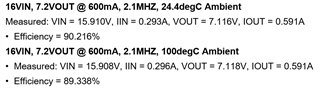
We measure LMR36015FSCQRNXTQ1 case temp at room temperature and would like to find out if running it at 80°C ambient would maintain junction temperature <150°C.

We follow two TI documents (LMR36006-Q1-thermal-case-study.PPT and Managing thermals with a 2-layer board deep dive).

We have the following questions:

  • In the PPT: "PLOSS at 100°C ambient is calculated" --> this seems to imply that PLOSS is the same at 100°C as it is at room temperature - is that a safe assumption?
  • The calculation in the PPT seems quite different from the one done in the deep dive". In the deep dive, how does one arrive at the 115°C max ambient in the last step (all previous steps are clear)?
  • Also, the LMR36006-Q1-thermal-case-study.PPT doesn't seem to remove the inductor DCR losses.
  • Bottom line, the two models  appear to give us a significant difference in projected Junction temperature. Which of the two is right?

Also: Since the thermal shutdown will only kick in at 170°C, what will happen between 150°C (max Junction temp) and 170°C?

Thanks much in advance,

gj

  • Hi gj,

    I am unfamiliar with LMR36006-Q1-thermal-case-study.PPT  as it's not on the LMR36006-Q1 product page. Could you post it?

    Thanks,

    Andrew

  • Hi Andrew, sorry, the URL seems to not have made it into my original post. LMR36006-Q1-thermal-case-study.PPT. It was shared by Marshall Beck in another thread in this forum. It was advertised as a good resource for determining the junction temperature of the LMR36015, which is why we used it. 

    regards, gj

  • Hi Guido,

    1. I don't think Marshall assumed that PLOSS was the same at 25C and 100C. That's why he measured efficiency at 25C and 100C. I think it's fair to say that efficiency may be a slightly worse at higher temps. You can always add extra margin at the end of your calculation if you are worried about small difference in losses.

    2. It seems like Sam extrapolated the the 115 degrees C number from how much hotter the junction is than 25C. From the video this is how I assume it's been calculated.

    22 (still air) + 28.4 (temp rise) = 50.4C

    150C (max temp) - 28.4 (temp rise) = 121.6 C max ambient 

    Afterwards, I think Sam reduced that 121.6 number to 115 in order to add margin for slightly lower efficiency at higher temps

    3. This is probably a small oversight. Technically you could remove those losses and have a higher margin for max operating temp.

    4. I think the video calculates the junction temperature incorrectly. I believe Sam should have used RθJC(top) instead of ψJT.

    5. To answer your question, likely the device may be damaged by thermal degradation before shutting off at 170C. I didn't design the part, but the mentality might be that functionality needs to be briefly maintained at high temperature in order to shut everything down properly.

    Thanks,

    Andrew

  • 1. I don't think Marshall assumed that PLOSS was the same at 25C and 100C. That's why he measured efficiency at 25C and 100C. I think it's fair to say that efficiency may be a slightly worse at higher temps. You can always add extra margin at the end of your calculation if you are worried about small difference in losses.

    OK. But that measurement at 100C never seems to have been used after this point. As we cannot reliably create an ambient of a high temperature here, we will estimate from the efficiency graphs in the datasheet.

    5. To answer your question, likely the device may be damaged by thermal degradation before shutting off at 170C. I didn't design the part, but the mentality might be that functionality needs to be briefly maintained at high temperature in order to shut everything down properly.

    OK.

    5. To answer your question, likely the device may be damaged by thermal degradation before shutting off at 170C. I didn't design the part, but the mentality might be that functionality needs to be briefly maintained at high temperature in order to shut everything down properly.

    OK.

    4. I think the video calculates the junction temperature incorrectly. I believe Sam should have used RθJC(top) instead of ψJT.

    Do you recommend to use the value from the datasheet (RθJC(top)=35.9°C/W)? I seem to recall from other documents that the use of the datasheet thermal parameters for design purposes was discouraged. But of course I'd be happy to go with it if the error is small.

    In the LMR36006/15 thermal case study mentioned earlier, they derived a PCB-specific Rθ using ΔT / PLOSS

    Would that not be more realistic compared to the generic JEDEC-RθJC(top) value from the datasheet?
     

    If I then put this together for our case it looks like this:

    LMR36015FSC junction temperature calcs.xlsx

    Would you kindly take a quick look over that to confirm it's correct? I did ignore the reduced efficiency at higher temperature. We are most interested in ensuring that we stay at a safe distance from max TJ. The given measurement is just an example. 

    ...

    The datasheet says "Thermal shutdown is provided to protect the regulator from excessive junction temperature". That sounds like it's intended to actually protect the device. I believe that is relevant for us as I am not very confident about the accuracy of the predicted junction temperature.

    A couple of more questions, if I may:

    • the deep dive video states "P_DISS_TOTAL =  5Vout*1.5Aout*(1-efficiency)" - shouldn't that be "P_DISS_TOTAL =  5Vout*1.5Aout*(1/efficiency - 1)"? Too late here, I can't see straight...
    • is there a known suited heat sink for this package?
    • Could the deep dive materials be corrected? Also, maybe the case study PPT that I pointed at earlier should be removed as well if it is incorrect.

    Thanks very much for your support!

    Kind regards,
    gj

  • Hi Guido,

    Do you recommend to use the value from the datasheet (RθJC(top)=35.9°C/W)? I seem to recall from other documents that the use of the datasheet thermal parameters for design purposes was discouraged. But of course I'd be happy to go with it if the error is small.

    In the LMR36006/15 thermal case study mentioned earlier, they derived a PCB-specific Rθ using ΔT / PLOSS

    Would that not be more realistic compared to the generic JEDEC-RθJC(top) value from the datasheet?

    Apologies for the confusion, but upon further thought, and looking at your excel I realize now that actually Marshall is actually just estimating the case top temperature at 100C operation. Sam measured the case top and then used ψJT (junction to case top) in order to calculate Tjunction. Marshall calculated Rθ and then multiplied losses by that Rθ to get case top at 100C.  

    Also as you mentioned, Marshall forgot to take into account DCR losses, so another ding toward him. 

    TAmbient target temperature: 80
    Case top temp   (°C) 65 measured
     Ambient temp (room temp)   (C°) 23 measured
    Vin  (V) 41.5 measured
    Iin  (A) 0.124 measured
    Vout  (V) 5.26 measured
    Iout  (A) 0.75 measured
    Efficiency 77%
     Ambient temp (room temp)   (C°) 80
    Vin  (V) - not measured
    Iin  (A) - not measured
    Vout  (V) - not measured
    Iout  (A) - not measured
    Efficiency 73% estimated, ignored
    PDISS_TOTAL   (W) 1.201 W
    PDISS_L   (W) 0.026 W
    PDISS_IC   (W) 1.175 W
    Thermal resistance, ψJT   (°C/W) 0.80 per datasheet
    Temperature increase  (°C) 0.94
    Junction Temperature,  TJ   (°C) 65.94
    TBuffer to max TJ  (°C) 10
    max TAmb to keep TJ < max TJ - Buffer  (°C) 97.06

    If you plug in ψJT rather than Rθ, you get that the max ambient temperature for your application is 97.06C which is a bit more reasonable than the answer you got earlier.

    The (1-efficiency) term is the percentage of losses, so it's correct. (ex 97% efficiency -> 3% losses).

    Now that we have arrived at the correct answer, I don't think we need a heat sink. Let me know if you still want one though.

    Yeah probably that ppt should be deleted. It caused a bit of confusion for you and me.

    Thanks,
    Andrew

  • Hi Andrew, 

    Thanks much again - we will go with this calculation now. Remaining concerns:

    1) As we will have some cases that may push the TJ quite high, we would really like to understand the thermal shutdown better. The datasheet suggests it's a functioning protection mechanism. Can you help us to get this confirmed or point us into the right direction?  

    2) For some corner cases we would like to check available heat sink options. Do you have any more info that you can share on this?

    regards,
    gj

  • Hi Guido,

    1. As the datasheet states The device stops switching and PGOOD goes low when the device reaches 170C, the device will turn on again at around 158C. It functions to protect the device from extreme heat damage, but you're right that long term exposure to temperatures above 150C may affect device functionality.

    2. Hmm I'm not sure I've ever recommended a heatsink for a device this small before. Thicker copper layers, more copper surface area, and lots of ground vias can help with sinking heat from the device. 

    Thanks,

    Andrew

  • Hi Andrew,

    1. Understood. If we can't get the question answered whether there will be full recovery (i.e., the device doesn't take permanent damage) after thermal shutdown, then so be it, but it sure would be an interesting bit of information :-)   

    2. The problem was relating to existing PCBs - as a temporary fix. But we couldn't find appropriate heat sinks, either. No worries.

    I'd love to close it here but one additional thing has popped up during the tests: 

    3. Two PCBs with identical components except for the type of LMR36015 used show very different temperatures under same load conditions. One uses LMR36015FSCQRNXTQ1 2.1 MHz FPWM, the other uses LMR36015SFBRNXR 1 MHz FPWM. Vin is 42V. The inductor is 6.8uH for both. Between 0.75A and 1.5A load, the measured case temperatures differ by 40-50°C. As both flavours are FPWM, this surprised us. Is there an obvious explanation for this?

    Regards,q
    gj

  • Hi Guido,

    Understood for 1 and 2.

    3. For this one, It doesn't surprise me that one is hotter than the other (50C does seem like a lot though). It has to do with how fast the device is switching. A higher switching frequency leads to higher L losses (both AC and DC), as well has internal MOSFET switching losses (energy builds up on the FETS similar to a capacitor each switching cycle. This energy gets released when the HSFET turns on, and there's more losses the more you switch.)

    To mitigate these losses on the higher switching frequency device, you could technically opt for a lower inductance with lower DCR. I really only recommend the higher switching frequency is a fast transient response is required for the application.

    Thanks,
    Adnrew

  • 3. Yes, we did expect some difference in temperature but the 40-50°C seems excessive. The inductor value on both PCBs was close to the value recommended for the 1 MHz version (6.8uH used, 8.5uH "typical" part, but far bigger than L_MIN as per data sheet). So that should work for both. 

    The efficiency plots at 1 MHz vs 2.1 MHz (checked LMR36015-Q1, LMR36015, LMR36015S) don't seem to suggest that this temperature difference should have anything to do with the efficiency. Any hints as to how we can proceed to find the root cause for the delta temp?

    Thanks again,
    gj

  • I'll check with the team and get back to you.

    Thanks,
    Andrew

  • Hi Guido,

    I looked into it, and I think the 2.1MHz part just runs hot. There are ways to sink the heat like adding more ground vias, or using a PCB with a large ground plane. Here's another person who pointed out the same issue you did.

    https://e2e.ti.com/support/power-management-group/power-management/f/power-management-forum/778184/lmr36015-q1-regulator-too-hot?tisearch=e2e-sitesearch&keymatch=LMR36015-Q1#

    Is there anything in your application that prevents you from using a lower switching frequency (like 400KHz)? I would suggest going with something like that.

    Thanks,
    Andrew

  • Andrew, thanks. 

    I agree with the other forum user's conclusion that the 2.1 MHz variant of the chip seems to have a problem. As I already said, this seems to clearly go beyond what can be explained with what the data sheet contains. 

    We will move to the 1 MHz part (but that also depends on the EMI signature) and provide more thermal relief in the design. But I think a clearer warning should be displayed to designers that this part behaves significantly more problematic thermally than its lower frequency family members. How about adding a plot with all chip variants showing chip temperature vs. load on a reference PCB? I would not recommend to use this part in an extended ambient temperature environment without being prepared to go to great lengths in the layout and having lots more board space available for cooling than the 10x16mm stated (e.g. on the eval PCB). 

    Thanks for your support + regards,
    gj