This thread has been locked.

If you have a related question, please click the "Ask a related question" button in the top right corner. The newly created question will be automatically linked to this question.

BQ77915: Schematic check request

Part Number: BQ77915
Other Parts Discussed in Thread: BQ76200, BQ76952, BQ76940, BQ77216

Hello Sir:

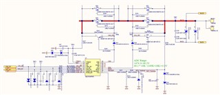
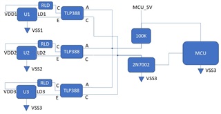
We have a project which is using 3pcs BQ77915 on our circuit.

Please help us to check our schematic.

That net "BQ 2nd CHG status" and "BQ 2nd DSG status" (in pdf schematic) are connected to our other circuits.

When "BQ 2nd CHG status" or "BQ 2nd DSG status" is high that net "CHG EN" or "DSG EN" (in jpg schematic) will be high. 

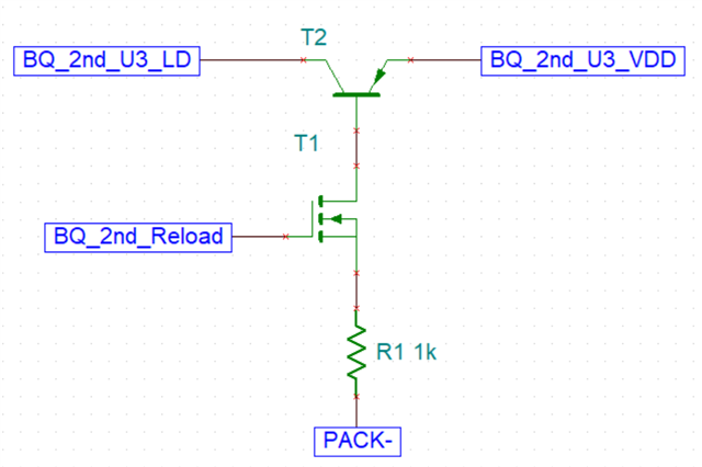
Especially that LD pin, we are using high side MOSFET, how to connect it? 

Looking forward your recommendations.

Thanks a lot.

BQ77915_stackable 3pcs.pdf

  • Hi Statham,

    Overall, your BQ77915 schematic looks good, though I have a couple corrections to make.

    First, under the assumption that you will only be connecting 3 cells to the top BQ77915 (hence the shorted cell inputs), you will need to short CCFG on just that device to its VSS. Please refer to Section 9.3.12 of the datasheet for an explanation of why.

    Next, R48 needs to change position. There should be no additional resistor between R46 and R29's common node and VSS. Instead, R48 should be placed from LD to VSS. Please refer to this application note which details stacked implementations, specifically figure 1-2 which shows the connections I have described.

    Also, the top of R49 needs to be connected to LD. Refer to the application note linked above, specifically figure 1-3 which shows this connection.

    Aside from those notes, your schematic appears to be correct.

    I am looping in a colleague to better assist you in checking your BQ76200 schematic.

    Regards,

    Max Verboncoeur

  • Hello Max:

    Thanks your assistance and recommendations.

    Please refer our updated version.

    DTF01_2nd Protected_V03.pdf

    By the way did you check LD pin? Our MOSFET is put on HIGH SIDE, and as my understanding that LD application note is for low side MOSFET application.

    Please let me know your recommendations on LD pin.

    Thanks a lot.

  • Hello Statham,

    On the B76200:

    I would recommend to add a resistor on the BJT collector side to control the FET turn-off speed. A 16-V Zener diode may also be desired in parallel to the gate-source resistors of the FETs (R195/R196). 

    A ~18-V Zener and a resistor may be good between the LD pin and the DSG. The reason for this is explained in Section 4.1 DSG Turn On of the bq76200 Beyond the Simple Application Schematic application note. I would recommend to read this application note.

    On the LD pin for the BQ77915:

    You are correct. The LD pin function may actually not work. Since LD would always be grounded to Vss, the device would essentially only recover based on time for OCD protections and may not be able to recover at all for OCC protection (since a positive voltage is required here). The conditions for OCD load removal is that the LD pin is below VLDT (~1.3-V), which would always be true for a high-side configuration. For the OCC protection, the condition to recover would be based if the LD pin is greater than VLDT. Which typically would never be the case here. So I do not believe the LD function would work at all in this case.

    Out of curiosity, what is the customer's application? Have they considered using the BQ76952? This device is a single-chip solution for up-to 16s cells that has integrated high-side FET drivers, autonomous cell balancing and a wide variety of protections. This device also incorporates a load-detect function that works for high-side too. This may be better for their application.

    Best Regards,

    Luis Hernandez Salomon

  • Hi Luis:

    Please refer below inf.

    1. I need to know if use high side MOSFET, how to connect LD pin? or how to ignore this function?

    2. Customer is using BQ76940 on their main protection, but some certification which needs to bypass main protection device, so we want to add Bq77915 on this certification.

    3. would you please help to check Bq77915 schematic again? 

    8838.DTF01_2nd Protected_V03.pdf

    Please let us know your recommendations.

    Thanks a lot.

  • Helllo Statham,

    1. I need to know if use high side MOSFET, how to connect LD pin? or how to ignore this function?
    I don't believe there is a good way to connect the LD pin. This device was not meant to be used high-side. The LD function is enabled in essentially all of our released parts. If connected to Vss, OCD/SCD would recover time based, and OCC will never be able to recover.

    If you are using a MCU, you may be able to control the LD pin by using it. So the MCU would have to be able to detect load/charger attachment and make decisions based on it.  

    2. Customer is using BQ76940 on their main protection, but some certification which needs to bypass main protection device, so we want to add Bq77915 on this certification.
    The BQ77915 is a primary protector, usually most customers need a secondary protector when redundancy is needed with a device like the BQ76940, which usually do OV/UV or temperature protections by driving a FUSE. Do they require a redundant secondary protector? Most customers also use a FUSE for this case.

    3. Would you please help to check Bq77915 schematic again? 
    I will let Max comment on the BQ77915 schematic.

    Best Regards,

    Luis Hernandez Salomon

  • Hi Statham,

    Aside from the special considerations for the LD pin to allow for high-side FETs, your schematic looks to be correct.

    The only change I would advise is for a stacked application that has shorted cells we recommend having the shorted cells on the lower devices so that the CTRD and CTRC signals from the higher devices are as strong as possible.

    In your case that would mean moving R24 to be in parallel with C16 rather than C2. This would also mean changing the CCFG configuration for both affected devices to match the change in cell configurations.

    Regards,

    Max Verboncoeur

  • Hi Luis and Max:

    Our customer updated the LD pin as below schematic.

    Would you please help to check it again?

    And let me know if there has any side effects.

    The other due to some mechanical issues, they want to use 5 series cell on U3, 4 series cell on U2 and 4 series cell on U1.

    Please let me know if there has any side effects. 

    Looking forward your feedback.

    Thanks a lot.

    DTF01_2nd Protected_newest.pdf

  • Hi Statham,

    It's probably fine to have the 4-series cell on the top device, the main reason to move it to the bottom is the stronger control signals, but if the signals are not an issue, then it's alright.

    As for the addition to the schematic for the LD pins, the customer has the right idea, but there are a few corrections and considerations to be made.

    If the customer does not need to have load-detection based recovery on the UV protection, then the solution is fairly simple (see below).

    If load-detection based UVP recovery is unnecessary then you can leave the LD pin on the upper devices floating and simply connect the device as shown above. The LD pin is internally pulled down, so leaving the BJT deactivated will simulate a disconnected load on the device. Activating the BJT by turning on the N-MOSFET will pull the LD pin up to VDD and simulate a load present on the device.

    We recommend against trying to do this on the other devices since the higher currents are potentially unsafe.

    If the customer does need load-detection based UVP then we would recommend looking at the BQ76952 to exchange for the BQ77915s and the BQ76200, since the BQ76952 supports up to 16 cells as well as high-side FETs.

    I hope this helps!

    Regards,

    Max Verboncoeur

  • Hello Max:

    Updated the newest version for you.

    Except the net BQ_2nd_CHG and R37, they didn't connect together. 

    LD pins had followed up your recommend.

    Please help to check it again.

    Looking forward your feedback.

    Thanks a lot.

    DTF01_2nd Protected_V05.pdf

  • Hi Statham,

    As I stated before, the circuit shown in my previous reply will only work with the bottom device in the stack, meaning you'll have to remove Q32 and Q33. After further consulting, having multiple BJTs connected together, like in this schematic, will result in some working as expected and others being always activated, defeating the purpose of the circuit.

    If the customer does not require the UV protection to recover based on load-detection, and only needs time-based recovery, then it is alright to leave the upper two devices' LD pin floating and to have only the one BJT on the lowest device's LD pin. You will still have normal operation with your current protections and can control their load recovery with the reload signal.

    If the customer requires load-detection based UVP then we recommend looking at the BQ76952 to exchange for the BQ77915's and the BQ76200, since the BQ76952 supports up to 16 cells, high-side FETs, and cell balancing, all in one device.

    Regards,

    Max Verboncoeur

  • Hi Max:

    Honestly, I don't understand why it can't recover from UVP.

    Because we are using High side MOSFET protection, and I only need to capture the CHG and DSG signals of 77915 to MCU.

    CHG and DSG will not be used as MOSFET drivers.

    So when any protection is activated (UV, OTD, OCC, OCD1/2 and SCD), LD voltage will always be VSS of each device.

    When I need to generate load removal behavior, do I just need to make a high to low transient on LD pin?

    That connect the LD pins of U1, U2 and U3 to the VDD of each device and it make a high transient,

    then disconnect all LD pins from VDD of each device and it make a low transient. 

    If the above is true, I can use an optocoupler to achieve.

    The optocoupler datasheet link shows below.

    https://www.mouser.tw/datasheet/2/408/TLP388_datasheet_en_20220518-1144548.pdf

    As shown below figure.

    Please let me know if I misunderstood?

    Or we don't care about the LD functions, can we use the same circuit on PRES pin?

    When I need to recovery, I just let PRES to floating then connect to high again and device will be recovery from any fault protections.

    Is it possible? Please let me know if I misunderstood?

    Looking forward your feedback.

    Thanks a lot.

  • Hello Statham,

    Most released parts require load removal for UV recovery. So, it will not recover unless the load is detected to be removed. 

    Why not use the BQ77216? This device is a 16s secondary protector that can show UV/OV faults and offers OW/Temperature protections. Only difference is that it does not have current protections. 

    So when any protection is activated (UV, OTD, OCC, OCD1/2 and SCD), LD voltage will always be VSS of each device.
    For these protections, if LD is at Vss the device would recover UV/OCD1-2/SCD, however, it would not recover in the event of a OCC protection. 

    An optocoupler may work, you just have to ensure that it remains low during UV/OCD/SCD protections, and it must go high if a OCC protection occurs to recover. 

    I do not know if HIBERNATE mode could recover from a fault. You may try this and see if it works, if this clears protections, that may also work. 

    Best Regards,

    Luis Hernandez Salomon