This thread has been locked.

If you have a related question, please click the "Ask a related question" button in the top right corner. The newly created question will be automatically linked to this question.

UCC28070: Some question about UCC28070

Part Number: UCC28070
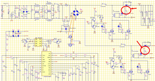
Other Parts Discussed in Thread: PMP40261

Dear Expert


1. The chip does not have AC undervoltage protection. After turning off AC, because the VCC of the chip is powered by an external auxiliary source, the chip will be fully driven after AC is turned off, making it impossible to achieve AC fast switching on and off. Therefore, an AC undervoltage circuit needs to be added to the periphery of the circuit;
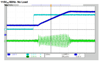
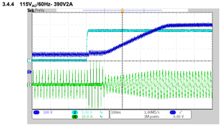
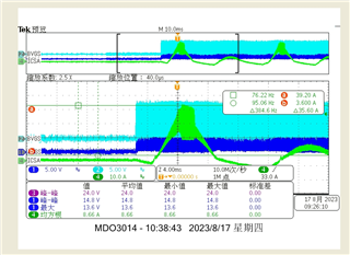
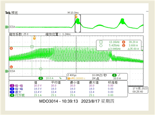
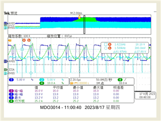
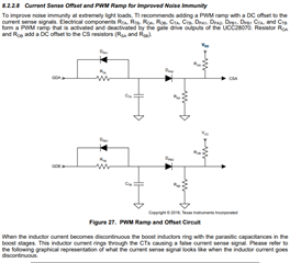
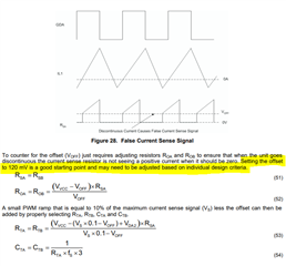
2. When switching the output power of PFC from 0W to 800W, the PFC current will reach the maximum current value of OCP at the moment of switching, and the chip will turn off the PFC drive, resulting in an abnormal current waveform;
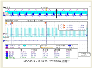
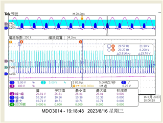
3. Is it normal for two different types of drives to occur when the output is unloaded and lightly loaded (0-60W), with one having more drives and the other not being driven at all? What modifications are needed to make the two drives consistent;
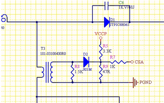
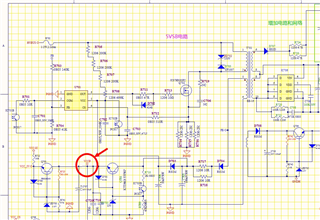
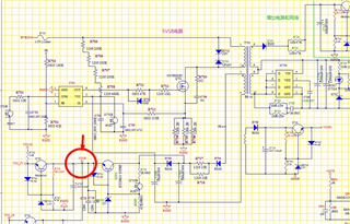
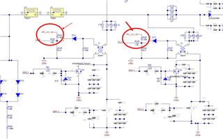
4. VCCP compensates for current sampling through R5, and what is the purpose of this compensation;

  • Hello Gabriel

    Question 1: The UCC28070 requires a bias supply for VCC but this supply does not have to be external. The PMP40261 reference design demonstrates this. Here, the UCC28070 bias uses a 12V rail from the current sense winding. There is also voltage protection for this 12V rail at startup. Thus, if the AC voltage is turned off, the UCC28070 will also turn off.

    Question 2: I am not sure what your question is. The PMP40261 also has a test report demonstrating the waveforms. The transients for 0W and 780W are shown below. So, if you switch from 0W to 780W you should get a transient response shown below and a current waveform in green.

    Question 3: Can you please clarify your question? GDA and GDB are clamped at 13.5V so you may need a gate driver for your PWM outputs. As an example, the UCC28070EVM shown below uses the UCC27324 gate driver. However, in the PMP40261 as shown above, the gate driver is replaced by a set of transistors. Functionally, they both provide the same purpose. 

    Question 4: Can you please share the schematic that your picture is from? I do not recognize the VCCP port.

    Regards,

    Jonathan Wong

  • Dear Jonathan

    Thanks for your reply ,but still customer have some question  .

    1.Reply: At present, the power supply method of VCC is provided by a flyback auxiliary source. When the input AC is turned off, HV is still working and the auxiliary source is still working. At this time, the VCC of UCC28070 is still maintained, and the phenomenon of UCC28070 fully driving occurs;
    As shown in Figure 1, the red circle represents the circuit provided by the flyback VCCP, while Figure 2 shows the circuit diagram of UCC28070. The red circle represents the VCCP, and this power supply comes from the VCCP position in Figure 1;

    Figure 1                                                                                             Figure 2

    2.Reply: The current waveform of PFC is abnormal during dynamic load operation, as shown in the following three pictures. When performing dynamic load operation with an output power of 10W-800W, the first current waveform of PFC will reach the set OCP point, causing the current waveform of PFC to be abnormal;
    Channel 1 is driven by CSA's MOS transistor VGS; Two channels are driven by CSB's MOS transistor VGS; 3 channels are the inductance L current waveform of CSA;


    Reply: The problem is that under light load, only one side is working, and CSA or CSB will drive and transmit energy, while the other side has no drive or the drive is very small; The following test waveform is the waveform with 30W:
    Channel 1 is driven by CSA's MOS transistor VGS; Two channels are driven by CSB's MOS transistor VGS; 3 channels are the waveform of the input voltage VAC;

    4.Reply: The position of VCPP comes from this place, stable at 12.3V, as shown in the following figure. What is the purpose of this position?

  • Hello Gabriel,

    Question 1: Yes, unfortunately the UCC28070 does not have a UVLO. You can try using an external UVLO circuit or by pulling the Soft Start pin low. However, the control loop for the UCC28070 is slow and thus you may only be able to switch at the AC line on and off around 1s.

    You may consider the UCC28019A since it offers UVLO and brownout

    Question 2+3: At low power the performance of the UCC28070 will be different. CSA or CSB may switch together or only one of them will switch. This is normal behavior and does not significantly affect the performance since this essentially turns the interleaved CCM into a single-phase CCM at low power.

    This PowerPoint below illustrates this behavior with our interleaved TM controllers but the concepts are the same for the interleaved CCM UCC28070.

    /cfs-file/__key/communityserver-discussions-components-files/196/Non_2D00_interleaving-Cases-with-UCC28061--UCC28063.pdf

    You also have an EMI filter at the input of the AC line. An EMI line filter is designed for the highest ripple at full power and has a constant inherent equivalent reactance. At high power this is insignificant since the PFC stage has a high equivalent impedance. However, at low power the PFC stage will have a lower equivalent impedance and the EMI filter will draw more current, thus affecting the performance.

    Question 4: The 12V rail applies a DC offset to the current sense. This is a technique to improve noise immunity since the inductor will operate in Discontinuous Conduction Mode (DCM) at light loads. You can view the design process on page 35 of the UCC28070 datasheet. 

    Regards,

    Jonathan Wong

  • Hi Gabriel,

    One idea to implement UVLO for the UCC28070 might be to use the TPS3701