This thread has been locked.

If you have a related question, please click the "Ask a related question" button in the top right corner. The newly created question will be automatically linked to this question.

LMR33620: Vout = Vin

Part Number: LMR33620
Other Parts Discussed in Thread: LMR33630

I had this issue on my prototype:

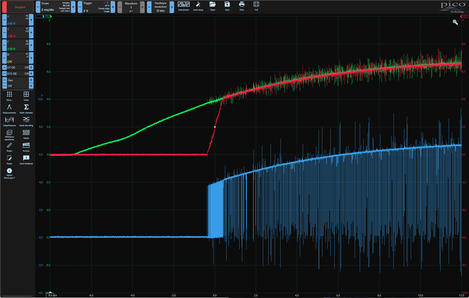
My LMR33620ARNX is switching at 140kHz with SW high 99.5% of the time. So Vout is close to Vin and FB is kept at 3V (when Vin=15V).

This was solved when I replaced the IC. But now I have got the production boards from the EMS and they all behave like the original prototype.

FB is not kept at 1V, I patched in a pull-up for PG and it is pulled low by the IC.

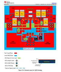
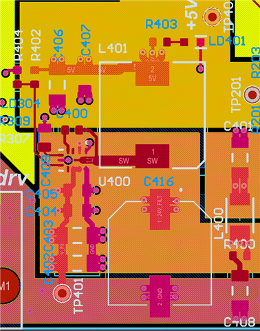
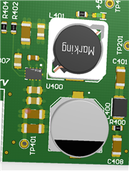
The layout is not according to the data sheet, but reasonably compact. GND plane (not shown) on layer 2, power polygons on layer 3.

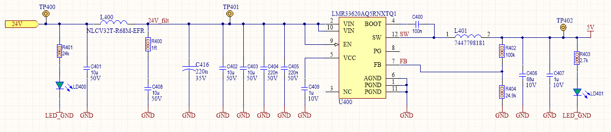
I have verified the values of C400 and C409 and tried adding some capacitance directly at FB pin but it did not help . Any ideas or suggestions what to try next?

  • Hello,

    I do not see any immediate issues with the schematic.

    For the layout, the feedback trace seems very long. The feedback trace should be as short as possible. Also, the input capacitance should be symmetric for this device, which the same amount of capacitance on each side. Here is an image of the datasheet layout for reference:

    I have the following questions:

    Are you seeing this behavior right away when the device is power on, or are you experiencing the issue after some time of operation?

    Do you have any voltage protection circuit on Vin to ensure that the absolute maximum voltage is not being violated?

    Best regards,

    Ridge

  • Hello Ridge,

    The behavior is there from startup (green Vin(7V), red Vout, blue SW):

    As you can see there is some changing of modes before it settles to 140kHz/99.5% duty cycle.

    There is no overvoltage protection (except filter and bulk cap), but the boards have only been powered with a soft start lab supply so far.

    I've also tried to add cap at the FB pin and lower the values of the voltage divider. Also tried patching in 100nF to pin 2 across the chip to GND of C405.

  • Hello,

    The feedback node needs to placed closer to the IC. As the layout is shown, you have a very long feedback trace and the feedback ground return is very far from the IC. Try moving the feedback resistors closer to the IC to reduce the size of the ground loop.

    What is your load when you observe this behavior?

    Best regards,

    Ridge

  • Hello,

    Moving the FB voltage divider to the FB pin did not help. I also tried minimizing SW-Boot loop area by wiring above NC pin as data sheet suggests but no success.

    I have tried loads from near zero up to 250mA, same behavior.

    Just saw that the chip is labeled 620AQ5, is this an automotive equivalent? My prototypes were labeled 33620A.

  • Hello,

    This behavior is reminiscent of the device operating in open loop, meaning the device does not have a feedback trace. Can you verify the soldering on some of your boards that you observe the issue on? Also, it seems like you are concerned with the parts. Can you provide the TI-approved vendor that you procured them from and a picture of the bag/reel label?

    It would also be good to provide a picture of the top mark of the IC.

    Best regards,

    Ridge

  • Hello,

    I've already inspected the soldering. And also tried to resolder all pins, though it's a bit tricky with 0.5mm VQFN.

    I can send an image of the top mark on Monday. I'm not really worried our EMS would buy from unofficial sources, rather if they bought a similar part number by accident. But I'll ask them for supplier and reel info if possible.

    Any chance this could be due to the inductor value/type? It is one of the types suggested by Webench, but just wondering.

  • Hello,

    I don't think the inductor is the problem. The part number listed on your schematic should be suitable.

    The waveforms you shared are reminiscent of a soldering or layout issue. You could try soldering a device form one of the problematic boards onto the EVM to see if it works: https://www.ti.com/lit/ug/snvu573a/snvu573a.pdf

    You can change out other parts on the EVM to more closely resemble your design if you need to as well.

    We will take a look at the information you mentioned when you send it to us.

    Best regards,

    Ridge

  • Hello,

    Here is an image of the package:

    Good to know there is an eval board for the LMR33630 (looked but didn't find one for the 33620). I might order one and try to swap the chip. But then if it doesn't work I would still be unsure about the soldering..

  • Hi,

    For this experiment, I think the LMR33630 should be sufficient. The only difference between the two products is the current limit. Adjust the EVM components to match your design and see if you can replicate the issue. Then, try replacing the chip on the EVM with the chips on your boards.

    If you are concerned with your ICs, we need the receipt and reel/bag sticker from the TI-approved vendor. The top mark does not give us the information we need check the IC information.

    Best regards,

    Ridge

  • The solution was ridiculously simple. For the prototype only the adjustable version was available. For the production boards I got the fixed 5V version. But in this case the voltage divider should have been replaced with a zero ohm resistor.