This thread has been locked.

If you have a related question, please click the "Ask a related question" button in the top right corner. The newly created question will be automatically linked to this question.

TPS25942A: Cout requirements

Part Number: TPS25942A
Other Parts Discussed in Thread: BQ25306, TPS25947, TPS25947EVM, LM5118

Hi,

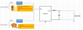
I want to use the TPS25942A eFuse IC to connect two external power sources/batteries  4S (12-16.8V) and 3S (9-12.6V) to the Li-Ion 2S battery charger BQ25306.

The external power source/batteries are connected only separately and mechanically protected to connect them simultaneously.

The connector pins of 4S (12-16.8V) are accessible to make a single point of failure when the 3S (9-12.6V) battery is connected.

When the 4S (12-16.8V) battery is connected the second battery 3S pins are covered and not accessible from a single point of failure.


System requirements:

Vin1= 4S (12-16.8V)

Vin2= 3S (9-12.6V)

Iin_max=2A

Have to support:

a. UVLO_1=12V and UVLO_2=9V

b. Reverse current protection 

c. OVP (TPS25306 has maximum operational Vin=17V)

d. OCP - is optional. It's supported by the Li-Ion 2S battery charger TPS25306

1. What is the TI IC's best option to support my requirements?

2. Could you please clarify why all eFUSE ICs have huge tantalum capacitors at the output 100uF?

3. Can I eliminate or use a small ceramic capacitor instead for my configuration that does not require energy storage? Is the BQ25306 Cin=2.2uF enough to serve the both BQ input and eFUSE output?

4.  What do you think, is my system assailable to the input hotplugging? or the charger (Li-Ion 2S battery charger BQ25306) turn-on activation time will delay the high charging current appearance and will nature eliminate the hotpluging phenomena? The input battery is connected with very short (~2cm) and thick wires.

Thanks

Vitaliy

  • Hi Vitaliy,

    Please see my response inline:

    1. TPS25942 can be used here. I will recommend TPS25947 which is latest device with better specs.

    2. Output cap is not mandatory to use. We only recommend small ceramic cap like 0.1uf for decoupling purpose.

    3.Yes that should be fine.

    4. eFuse has inrush current control which protects system from high current due to hot-plugging. 

    Regards

    Kunal Goel

  • Hi Kunal,

    Thanks for your answers and proposal.

    Please see TPS259470ARPW_Design_Calculator.xlsm attached

    TPS259470ARPW_Design_Calculator.xlsm

    1. Could you please clarify the meaning of the UV threshold set-up?

    To prevent the "dead" (deep discharge) battery as used as the input source, I would like to set up UV_final_falling = 12V (4S Li-Ion battery pack with minimum operation voltage 3V*4=12V).

    So, if the input battery voltage is dropped to 12V, the UV mechanism will shut down the eFUSE to protect the battery from deep discharging. The load current disconnection will cause the battery OCV to rise and then UV_final_rising=13V will prevent the eFuse undesired power ON/OFF loop till the IC sees the stable input voltage above the UV_final_rising=13V.

    What will happen during the First input source battery attached with OCV voltage below UV_final_rising=13V? Does the eFuse keep OFF and turn ON ONLY above UV_final_rising? Will the input source insertion allow the eFuse start-up operation only above the UV_final_rising=13V?

    According to the _Design_Calculator.xlsm 

    I have to set UVLO set point = 13.3V!!! in .xlsm to get the UV power fail (Vin falling) threshold at 12.03V.

    The release of UVLO (Vin Rising) will have occurred at 13.12V.

    Does it seem correct?

    2. I have set "Load turn on voltage" = 12V Come back to my previous UV setup it should be 13.12V? Correct?

    I can't see in the spreadsheet what are the parameters affected by this value.

    Thanks

    Vitaliy

  • Hi Kunal,

    Could you please clarify what is the reason for PGNDX and GNDX separation on TPS25947EVM?

    Is it shorted finally with NT1/2/3/4 Net-Tie on the PCB level?

    Regards

    Vitaliy

  • Hi Vitaliy,

    Yes they are shorted finally with NT. 

    The GND terminal must be tied to the PCB ground plane at the terminal of the IC with the shortest possible trace. The PCB ground must be a copper plane or island on the board. TI recommends to have a separate ground plane island for the eFuse. This plane doesn't carry any high currents and serves as a quiet ground reference for all the critical analog signals of the eFuse. The device ground plane must be connected to the system power ground plane using a star connection.

    Regards

    Kunal Goel

  • Hi Kunal,

    Have you missed my previous question? 

    Sorry, I've sent two in a row.

    Hi Kunal,

    Thanks for your answers and proposal.

    Please see TPS259470ARPW_Design_Calculator.xlsm attached

    TPS259470ARPW_Design_Calculator.xlsm

    1. Could you please clarify the meaning of the UV threshold set-up?

    To prevent the "dead" (deep discharge) battery as used as the input source, I would like to set up UV_final_falling = 12V (4S Li-Ion battery pack with minimum operation voltage 3V*4=12V).

    So, if the input battery voltage (discharging) is dropped to 12V, the UV mechanism will shut down the eFUSE to protect the battery from deep discharging. The load current disconnection will cause the battery OC voltage to rise and then UV_final_rising=13V will prevent the eFuse undesired power ON/OFF loop till the IC sees the stable input voltage above the UV_final_rising=13V.

    What will happen when the First input source battery is attached with OCV voltage below UV_final_rising=13V? Does the eFuse keep OFF and turn ON ONLY above UV_final_rising? Will the input source insertion allow the eFuse start-up operation only above the UV_final_rising=13V?

    According to the _Design_Calculator.xlsm 

    I have to set UVLO set point = 13.3V!!! in .xlsm to get the UV power fail (Vin falling) threshold at 12.03V.

    The release of UVLO (Vin Rising) will have occurred at 13.12V.

    Does it seem correct?

    2. I have set "Load turn on voltage" = 12V Come back to my previous UV setup it should be 13.12V? Correct?

    I can't see in the spreadsheet the parameters affected by this value.

    Regards

    Vitaliy

    TPS259470ARPW_Design_Calculator.xlsm

  • Hi Vitaliy,

    Sorry I missed your question. 

    1.Yes input voltage has to be above UV rising threshold to enable the eFuse. 

    2. What will happen when the First input source battery is attached with OCV voltage below UV_final_rising=13V? eFuse will not turn on.

    3. Does the eFuse keep OFF and turn ON ONLY above UV_final_rising? Yes

    4. Will the input source insertion allow the eFuse start-up operation only above the UV_final_rising=13V? Yes

    5. Load turn on voltage means voltage at which your load gets enabled. We have kept it in calc to help in startup calculations. It can be less than VIN. 

    Regards

    Kunal Goel

  • Hi Kunal,

    Thanks.

    Could you please share the secure link for the schematic and implementation review?

    Regards

    Vitaliy

  • Hi Vitaliy,

    We can discuss on e2e private messaging.

    Regards

    Kunal Goel

  • Hi Kunal,

    We plan to connect two external batteries, one with 3S and the other with 4S, as input sources to the 2S charger of BQ25306. This will be done through two ORing eFuses TPS259470A. The two input batteries will always remain connected separately, which means one eFuse path will always stay unpowered. To ensure this, we planned to use the AUXOFF pins to disable the BQ25306 charger via the EN pin while the active eFuse protection like OV/UV/Reverse V&I.

    I have a plan to use an external 3.3V LDO and a single PU 100k on AUXOFF1 & 2, connected to the EN pin of BQ25306. However, I tested it today on TPS25947EVM and found out that the AUXOFF OD pin on the unpowered path affects the output voltage due to the internal sink current into the AUXOFF pin.

    The AUXOFF Vout varies between 0.58V (1M), 0.68V (100k) and 0.78V (10k) depending on the PU value. Therefore, the unpowered path cannot allow simple BQ25306 EN control by AUXOFF1&2 Oring or via the Shottky Oring due to Vout. 

    From the Spec:  there is no active pull-down in this condition to drive this pin down to 0 V. If the AUXOFF pin is pulled up to an independent supply which is present even if the device is unpowered, there can be a small voltage seen on this pin depending on the pin sink current, which is a function of the pull-up supply voltage and resistor. Minimize the sink current to keep this pin voltage low enough not to be detected as a logic HIGH by associated external circuits in this condition. 

    PG/AUXOFF pin voltage while de-asserted. VIN < VUVP(F), VEN < VSD(F), Weak pull-up (IPG = 26 μA)    - 0.67V

    PG/AUXOFF pin voltage while de-asserted, VIN < VUVP(F), VEN < VSD(F), Strong pull-up (IPG = 242 μA)  - 0.79V

    I can see two options to reduce the AUXOFF Vout 0.58-0.78V below the Vil < 0.4V. The first option is to OR it (common anode) via the rectifier diodes. The second option is to use an additional N-Channel inverter stage that is connected to the EN pin with Vgs_th high > 1-1.5V.

    Do you have any ideas on how I can accommodate these AUXOFF pins on both powered and unpowered paths for proper BQ25306 EN pin control during active protection events?

    How can I Minimize the sink current into the AUXOFF pin on the unpowered IC suggested by the specification? To use very high PU > 1M?

    The schematic is attached to the e2e private messaging chat. The common block diagram is attached to this thread earlier.

    Regards

    Vitaliy

  • Hi Vitaliy,

    I agree with your ideas. We can try increasing pull up impedance to make it go low.  Another idea maybe to create a resistor divider at AUXOFF pin by connecting a resistor from AUXOFF to GND. 

    Regards

    Kunal Goel

  • Hi Kunal,

    Our second configuration uses the same two external batteries connected through the two eFused to the RF PA Amplifier board now.

    The PA board has very big input and output capacitors for the Boost regulator to 50V LM5118. The PA itself has bias voltage but no RF signal and its current drain is only 0.5A.

    I have tried to simulate this configuration on TPS25947EVM - vai the VIN2 and VIN1 but can manage the normal eFuse power ON process for all operation Vin voltages from 10V - 17V.

    Please see my setup, configuration changes and test results slides attached. I plan to use eFuse TPS259470ARPW with Active Current Limit & Auto-Retry functions, which did not exist on the EVB. So, I've tried to simulate my final configuration on the EVB.
     

    1. Can you please confirm the reason that eFuse is shutdown on TPS25947EVM - VIN2 
    TPS259470LRPWT with Active Current limiting & Latch-Off features for VIN > 12V and up to 17V?

    2. Does it make sense that a big capacitor on dV/dT caused the slow slew rate control while keeping a big voltage drop on internal eFuse FET’s (17V-6V) * ILIM (2.5-3A)=27-33W? and caused the Overtemperature event?

    3. Do you think the Auto-Retry feature be able to manage the normal eFuse power-up by sequentially supporting all inrush current spikes for all Vin's?

    7752.eFuse evaluation results and questions.ppt

    Kunal, Can we have a short call to clarify the results and possible options?

    Thanks

    Vitaliy