This thread has been locked.

If you have a related question, please click the "Ask a related question" button in the top right corner. The newly created question will be automatically linked to this question.

TPS92620-Q1: About PWM signals and output current

Part Number: TPS92620-Q1
Other Parts Discussed in Thread: TPS92633, TPS92633-Q1

Hi Sir,

My customer has the below questions about the TPS92620-Q1.

At the PWM signals 30Hz(33ms) and the high level of 1ms, could the TPS92620-Q1 be used for this PWM condition? 

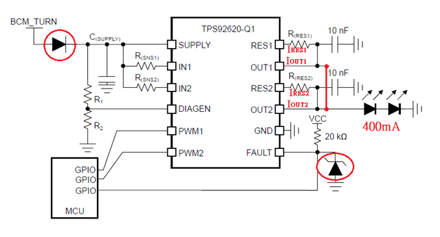
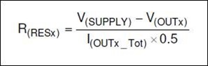
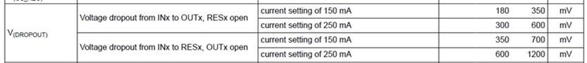
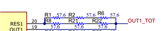
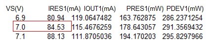
V-in = 12V(wide V-in = 5~36V), V-out =3.1V, I-out = 400mA. For output current condition, could they use TPS92620-Q1 2-ch in parallel to be 1-ch?

  • Hi Henry,

    1) Yes, this device can support this PWM duty cycle.

    2) Yes, you can parallel 2-ch as 1-ch.

    BR,

    Hailee.

  • Hi Sir,

    My customer wants that even during the disable of the TPS92620-Q1, the device also can report the LED open fault, right?

  • Hi Hailee,

    TPS92620-Q1 datasheet , 7.1 overview said that PWMx pins with frequency above 100Hz to adjust the LED brightness. If I apply 30Hz (different duty) to control on off in PWMx pin for CMOS sensor exposure , is it workable ?

    BR,

    joseph.

  • Hi Joseph,

    The 100Hz is mainly for visible frequency range of human eyes. 

    The customer can use lower frequencies based on specific requirements.

    BR,

    Hailee.

  • Hi Henry,

    What do you mean "disable the TPS92620-Q1"? PWM off or SUPPLY off? 

    BR,

    Hailee.

  • Hi Hailee,

    from TPS92620 datasheet (Figure 7-3 , 7.4) show the FAULT will not react if PWMx high interval is shorter than detection deglitch time (t6/125us and t7/125us)

    is it correct ?

    BR,

    joseph.

  • Hi Sir,

    Disable the TPS92620-Q1 for supply off.

  • Hi Henry,

    I am afraid that this device can't support off-supply open-load diagnostic.

    When SUPPLY is off, the function of diagnostic would be disabled.

    BR,

    Hailee.

  • Hi Joseph,

    Yes, you are correct.

    It needs the deglitch time to assert a true fault.

    BR,

    Hailee.

  • Hi Hailee,

    TPS92620 datasheet show that there is diode in supply pin input side.

    what is the purpose of this diode ?

    It also show a zener diode in FAULT output in , what is the purpose of this zener ?

    thanks.

    joseph.

  • Hi Hailee,

    My application is using two channel to drive 2LED (in serial) with 400mA

    each channel set 200mA output

    IOUT1=100mA , IRES1=100mA

    IOUT2=100mA , IRES2=100mA

    Is it ok with two channel to drive one LED connection and is it correct of IOUTx=IRESx=100mA ?

    or the max. current in IRESx will be 200mA ?

    (I have to consider the power rating of the R(RESx) resistor)

    thanks.

    joseph.

  • Hi Haliee,

    We will put a DC-2-DC to buck 12V to 7V first for TPS92620 driver power , to minimize the dropout voltage

    In this case , could the R(RESx) not exist (no mount) ?

    I have upload the circuit , which has R(RESx) exist case , and the circuit has including a DC-2-DC before TPS92620 power source, and with some calculation value inside.

    would you please support to check if there is any concern.

    question.

    1. should we add a diode in SUPPLY input pin side ?

    2. should we add a zener diode in FAULT output pin side ?

    3. could we remove the R(RESx) resistor in out circuit ?

    4. does the resistor value setting based on our calculation ok ?

    thanks.

    BR,

    joseph.

    TPS92620 SCHEMATIC 0111.pdf

  • Hi Joseph,

    The diode in SUPPLY pin is used to protect the power.

    The Zener diode in FAULT pin is used to protect the external MCU I/O pin.

    BR,

    Hailee.

  • Hi Joseph,

    What is the voltage level of this I/O? 

    BR,

    Hailee.

  • Hi Sir,

    Below are questions in the same project.

    Vsupply = 7V, Vinx =7V - 0.15V = 6.85V.
    IF_LED = Iout, total = 0.2A.
    VF_LED = Voutx = 4.5V at 85℃, = 5.0V at 25℃, = 5.5V at -20℃.

    Following Equation 9, to get the Rres = 25ohm (if VF_LED = 4.5V)
    So, VRESx = 4.5V + (0.2A/2)*25 ohm = 7V


    According to the below table in the datasheet, does it mean that when Vsupply rises to 9V ((Vsupply – VRESx) = 2V > 1V) more than 95% of Iout(0.2A) will flow through Rres?


    If the environment temperature is -20℃ (VF_LED = 5.5V)
    VRESx = 5.5V + (0.2A/2)*25 ohm = 8V, VRESx > Vsupply(7V).
    Vsupply – VRESx = -1V.
    Vsupply – Voutx = 7V – 5.5V = 1.5V


    Does it cause IRESx to become smaller and IOUTx to become larger?
    Is there any formula to calculate IRESx and IOUTx at -20℃?
     

    In addition, following Equation 9, we need to select which Voutx value (4.5V, 5.0V, or 5.5V) to calculate Rres?

  • Hi Hailee,

    /FAULT is signal is output from TPS92620 through a NMOS to go into a Serializer IO pin. The /FAULT is active high 1.8V level

    thanks.

    BR,

    joseph.

  • Hi Joseph, 

    1. Even you put a Buck in front of this IC, I still want to recommend you keep the RES resistor.

    Or maybe you can remove the buck and use more RES resistors (as shown below, the rated power of the RES resistor can be smaller) to share more power from the device. 

    The selection of RES resistor is a trade off between the power of RES resistors and the device.

    2. Yes, It is recommended to add one.

    3. From my understanding, for FAULT signal, do you want to achieve the logic -

    when the FAULT pin is high, the /FAULT is low; and when the FAULT pin is low, the /FAULT is high?

    4. For RES, this value is okay when the SUPPLY voltage is 7V, or you can use 50//50 to replace R444(24.9R 2520) for reducing the rated power of the Rres.

    For DIAGEN pin, it is recommended that you select R452 with a value close to 43.35ohm to match the voltage range of VIHDIAGEN and enable the OPEN diagnostic.

    BR,

    Hailee.

  • Hi Henry,

    The current in the RES path and OUT path is not constant under different voltage conditions.

    TPS92633-Q1 and TPS92620 are similar and they have the same function - thermal sharing. Please refer to the calculation tool of TPS92633 on ti.com and you can see the current change in the RES path and OUT paths at different SUPPLY voltage, output voltage and RES resistance. 

    TPS92633-Q1 data sheet, product information and support | TI.com

    BR,

    Hailee.

  • Hi Sir,

    Vsupply = 7V , Vout = 4.5V, Ioutx_total = 200mA.
    Following TPS92620 datasheet equation 9 to calculate the value of Rres, the result for Rres is 25 Ohm.

    We used the RES resistor page on the calculation tool of TPS92633, and input the below values.
    Vcs_reg =150mV (TPS92620 typical value), Iout_tol = 200mA, Vout = 4.5V, Rres = 25 Ohm.

    Why the Ires value is 84mA at VS(V) is 7.0V, but it is not 100mA? the customer needs the IOUTx = 100mA , IRESx = 100mA.

  • Hi Henry,

    The equation 9 is based on an ideal situation. Users can set different RES resistors according to their voltage and current requirements.

    If the customer wants to achieve IOUTx=100mA, IRESx=100mA, the resistance of the RES resistors can be reduced to 20~21Ω.

    Please refer to the below tool.

    TPS92620-Q1 External Components Calculation Tool-Rev1.xlsx

    Many thanks!

    BR,

    Hailee.

  • Hi Sir,

    Many thanks for your provided file.

    In the functional block diagram, we can find the VCC.
    Does it mean the bias supply voltage? How much voltage is it?

  • Hi Henry,

    The Fault output voltage could be constant within the range of 6~7V when SUPPLY voltage is higher than this value.

    You can test the EVM board and see the changes.

    Many thanks!

    BR,

    Hailee.

  • Hi Sir,

    Could you please help to review the schematics and advise comments? Thanks!

    TPS92620 SCHEMATIC 0122.pdf

    If the customer removed the buck converter and used 6~28V-in DC power input directly.

    The design Requirements: Vout 1= Vout2 = 5V, Iout1 = Iout2 = 200mA, at TA = 95C.

    How to calculate the resistance value of RES1 and RES2? since they are concerned the IC has a thermal shutdown issue at TA=95C.

  • Hi Henry,

    Please give some time, and I will get back to you within 24 hours.

    Many thanks!

    BR,

    Hailee.

  • Hi Henry,

    1) From my side, we need to consider the thermal performance under the worst case - Vout1 =4.5V.

    I'd like to recommend that you increase the value of the RES resistors to 30Ω for each channel. (10Ω + 10Ω +10Ω)

    2) The voltage range 6~28V is a bit wide, what is this application and what is the typical voltage? 

    BR,

    Hailee.

  • hi, Hailee:

       Thanks for your comment.

       I have  questions , Is 30ohm for our current schematic (including DC to DC)?

     , and is 30ohm (10ohm*3) based on the power rating of the resistors, or is it due to the thermal balance between the IC and the resistors?

       Because our PCB area is insufficient, can we use 15ohm+15ohm for 30ohm?

      The voltage is 6~28V because the customer has tested that the car battery can maintain operation at both the high voltage of 26V and the low voltage of 6V.

    Thanks.

    Dylan.

  • HI henry,

    • Sorry for the misunderstanding, the recommendation of 30ohm is due to the thermal balance between the IC and the RES resistors when supply voltage is high and to increase the power shared by the RES resistors. For your current schematic, if the supply voltage is 7V, 20ohm would be ok.
    • The dropout voltage of the device would be very high when Vsupply is 26V. if the device works under this condition for a long time, the thermal would be a big concern. but from my side, I think this voltage range is a test item, right?  what is the test time requirement? and what is the normal operating voltage? 

    Many thanks!

    BR,

    Hailee.