This thread has been locked.

If you have a related question, please click the "Ask a related question" button in the top right corner. The newly created question will be automatically linked to this question.

Why my automated programming with TPS6594 doesn't work

Hi,

I'm trying to automate the programming of TPS6594 with Python, but it seems not working. These are the findings when I compared my automated programming with the programming by Scalable PMICs GUI.

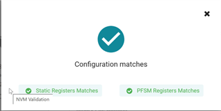
1. All the NVM values are stored in a bin file. After I programmed with Python, I was able to use Scalable PMICs GUI to validate that the NVM settings matched the values specified in the bin file. 

2. This the definition of the PFSM with Scalable PMICs GUI:

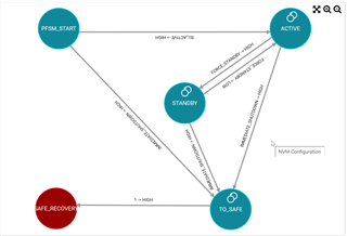
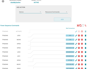
3. When I programmed with my Python script, I checked the register map with the GUI, and I found that LDO2 is not enabled as required in the ACTIVE state, and the LDO2 CTRL register (at 0x001e) has value of 0x02, which, according to the datasheet , means the LDO2 regulator is disabled. So I checked the .bin file, and I found the register value at address is defined to be 0x02, which matches the value in the register map.

4. When I programmed it with PMIC GUI with the same .bin file, everything works. However, the LDO2 CTRO register has the value of 0x13, which means the regulator is enabled. Although the chip works, the register value at LDO2 CTRL doesn't match the definition in my bin file. Why is that? Was it because there was state transition that happened after the programming?

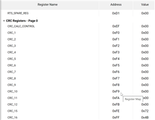
5. I also found the PMICs GUI would write to all the CRC Registers (CRC_1 ~ CRC_16), while my Python script wouldn't program all of them but only CRC_15 and CRC_16, as shown in the figure below. Are the CRC registers CRC1~CRC_14 are necessary to be programmed for the chip to work properly?

So my additional questions are below:

1. Why does my script seem to have programmed the correct values to the NVM, but TPS6594 is not working/active?

2. Do I need to issue any other commands to make it start?

3. Do you have any sample python script that could program it?

Thank you very much!

  • I dug into the values of registers 0x5A, 0x67, 0x69, and 0x6C, and found they have the following values:

    0x5A: 0xA8

    0x67: 0x0C

    0x69: 0x01

    0x6C: 0x00

    From the values of register 0x67, the "REG_CRC_ERR_INT" was set, why is that since I didn't enable the CRC?

    From the values of register 0x69, it indicates there is a "IMM_SHUTDOWN_INT". It seems the over voltage protection was triggered based on the comments from the below link:

    e2e.ti.com/.../tps6594-q1-difference-between-pmic-immediate-shutdown-orderly-shutdown-mcu-power-error

    But how do I check further which voltage protection was triggereed?

    Thanks!

  • So I checked the .bin file, and I found the register value at address is defined to be 0x02, which matches the value in the register map.

    In the .bin file, addresses below 0x3000 represent the static registers. These are the values when the NVM is first loaded but don't represent the value that the PFSM may change something to. In the case of LDO2, the step that enables the rail in the power up sequence would be in the PFSM registers. (0x3000 - 0x32FF).

    I also found the PMICs GUI would write to all the CRC Registers (CRC_1 ~ CRC_16), while my Python script wouldn't program all of them but only CRC_15 and CRC_16, as shown in the figure below. Are the CRC registers CRC1~CRC_14 are necessary to be programmed for the chip to work properly?

    Yes, this means a state transition occurred.

    Are the CRC registers CRC1~CRC_14 are necessary to be programmed for the chip to work properly?

  • I dug into the values of registers 0x5A, 0x67, 0x69, and 0x6C, and found they have the following values:

    0x5A: 0xA8

    0x67: 0x0C

    0x69: 0x01

    0x6C: 0x00

    From these values, it does not appear to have been an over voltage event. The register crc error is the primary fault. 

  • Do you have any sample python script that could program it?

    We have example C code that uses MSP432 to program the device. 

    programTP6594Example.c
    /* --COPYRIGHT--,BSD
     * Copyright (c) 2017, Texas Instruments Incorporated
     * All rights reserved.
     *
     * Redistribution and use in source and binary forms, with or without
     * modification, are permitted provided that the following conditions
     * are met:
     *
     * *  Redistributions of source code must retain the above copyright
     *    notice, this list of conditions and the following disclaimer.
     *
     * *  Redistributions in binary form must reproduce the above copyright
     *    notice, this list of conditions and the following disclaimer in the
     *    documentation and/or other materials provided with the distribution.
     *
     * *  Neither the name of Texas Instruments Incorporated nor the names of
     *    its contributors may be used to endorse or promote products derived
     *    from this software without specific prior written permission.
     *
     * THIS SOFTWARE IS PROVIDED BY THE COPYRIGHT HOLDERS AND CONTRIBUTORS "AS IS"
     * AND ANY EXPRESS OR IMPLIED WARRANTIES, INCLUDING, BUT NOT LIMITED TO,
     * THE IMPLIED WARRANTIES OF MERCHANTABILITY AND FITNESS FOR A PARTICULAR
     * PURPOSE ARE DISCLAIMED. IN NO EVENT SHALL THE COPYRIGHT OWNER OR
     * CONTRIBUTORS BE LIABLE FOR ANY DIRECT, INDIRECT, INCIDENTAL, SPECIAL,
     * EXEMPLARY, OR CONSEQUENTIAL DAMAGES (INCLUDING, BUT NOT LIMITED TO,
     * PROCUREMENT OF SUBSTITUTE GOODS OR SERVICES; LOSS OF USE, DATA, OR PROFITS;
     * OR BUSINESS INTERRUPTION) HOWEVER CAUSED AND ON ANY THEORY OF LIABILITY,
     * WHETHER IN CONTRACT, STRICT LIABILITY, OR TORT (INCLUDING NEGLIGENCE OR
     * OTHERWISE) ARISING IN ANY WAY OUT OF THE USE OF THIS SOFTWARE,
     * EVEN IF ADVISED OF THE POSSIBILITY OF SUCH DAMAGE.
     * --/COPYRIGHT--*/
    /*******************************************************************************
     *  MSP432 I2C - EUSCI_B0_BASE I2C TX multiple bytes to Secondary
     *
     *  Description: This demo uses I2C of the MSP to program the
     *
     *                                /|\  /|\
     *                MSP432P4111      10k  10k
     *                   slave         |    |
     *             -----------------   |    |
     *            |     P1.6/UCB0SDA|<-|----+->
     *            |                 |  |
     *            |                 |  |
     *            |     P1.7/UCB0SCL|<-+------>
     *            |                 |
     *
     *
     *
     ******************************************************************************/
    /* DriverLib Includes */
    #include <ti/devices/msp432p4xx/driverlib/driverlib.h>
    
    #include <tps6594BinSource.h>
    
    #define STARTINGPAGE0_ADDRESS   0x48
    
    /* Register Addresses */
    #define DEVICE_ID               0x0001
    #define NVM_ID                  0x0002
    #define NVM_REV                 0x0003
    #define CRC_1                   0x00F0
    #define CRC_2                   0x00F1
    #define USER_EE_CTRL_1          0x00A2
    #define USER_EE_CTRL_2          0x00A3
    #define MASK_INCLUDE            0
    #define MASK_EXCLUDE            1
    #define PAGE1_I2C1_OFFSET       34
    #define PAGE1_I2C2_OFFSET       35
    #define ENDRV_STAT_OFFSET       3
    #define ADDRESS                 0
    #define DATA                    1
    #define REG_CRC_EN_OFFSET       0x0018
    
    uint8_t page0_I2C_addr;
    
    const uint8_t userDataCRC_mask[256][2] =
    {
        {0x00, 0x00},
        {0xFF, 0xFF},
        {0xFF, 0xFF},
        {0xFF, 0xFF},
        {0xFF, 0xBF},
        {0xFF, 0x3F},
        {0xFF, 0xBB},
        {0xFF, 0x3F},
        {0xFF, 0xBF},
        {0xFF, 0x3F},
        {0xFF, 0xBB},
        {0xFF, 0x3F},
        {0xFF, 0xFF},
        {0xFF, 0xFF},
        {0xFF, 0xFF},
        {0xFF, 0xFF},
        {0xFF, 0xFF},
        {0xFF, 0xFF},
        {0xFF, 0xFF},
        {0xFF, 0xFF},
        {0xFF, 0xFF},
        {0xFF, 0xFF},
        {0xFF, 0xFF},
        {0xFF, 0xFF},
        {0xFF, 0x3F},
        {0xFF, 0x3F},
        {0xFF, 0x3F},
        {0xFF, 0x3F},
        {0xFF, 0xF3},
        {0xFF, 0xF3},
        {0xFF, 0xF3},
        {0xFF, 0xF3},
        {0xFF, 0xFF},
        {0x00, 0x00},
        {0xFF, 0x01},
        {0xFF, 0xFE},
        {0xFF, 0xFE},
        {0xFF, 0xFE},
        {0xFF, 0x7F},
        {0xFF, 0x3F},
        {0xFF, 0x3F},
        {0xFF, 0x3F},
        {0xFF, 0x3F},
        {0xFF, 0x21},
        {0xFF, 0x7F},
        {0x00, 0x00},
        {0x00, 0x00},
        {0x00, 0x00},
        {0x00, 0x00},
        {0xFF, 0xFF},
        {0xFF, 0xFF},
        {0xFF, 0x10},
        {0xFF, 0x10},
        {0xFF, 0xFF},
        {0xFF, 0xFF},
        {0xFF, 0xFF},
        {0xFF, 0xFF},
        {0xFF, 0xFF},
        {0xFF, 0xFF},
        {0xFF, 0xFF},
        {0xFF, 0x11},
        {0xFF, 0xFF},
        {0xFF, 0x07},
        {0x00, 0x00},
        {0x00, 0x00},
        {0xFF, 0xFF},
        {0xFF, 0xFF},
        {0xFF, 0x0F},
        {0xFF, 0xFF},
        {0xFF, 0x03},
        {0xFF, 0xFF},
        {0xFF, 0xFF},
        {0xFF, 0x3F},
        {0xFF, 0xBB},
        {0xFF, 0xBB},
        {0xFF, 0x0B},
        {0xFF, 0xBB},
        {0xFF, 0xBB},
        {0xFF, 0x03},
        {0xFF, 0xF3},
        {0xFF, 0xF3},
        {0xFF, 0x3F},
        {0xFF, 0x20},
        {0xFF, 0x0B},
        {0xFF, 0xD6},
        {0x00, 0x00},
        {0xFF, 0x0F},
        {0xFF, 0xAB},
        {0xFF, 0x09},
        {0xFF, 0x3F},
        {0x00, 0x00},
        {0x00, 0x00},
        {0x00, 0x00},
        {0x00, 0x00},
        {0x00, 0x00},
        {0x00, 0x00},
        {0x00, 0x00},
        {0x00, 0x00},
        {0x00, 0x00},
        {0x00, 0x00},
        {0x00, 0x00},
        {0x00, 0x00},
        {0x00, 0x00},
        {0x00, 0x00},
        {0x00, 0x00},
        {0x00, 0x00},
        {0x00, 0x00},
        {0x00, 0x00},
        {0x00, 0x00},
        {0x00, 0x00},
        {0x00, 0x00},
        {0x00, 0x00},
        {0x00, 0x00},
        {0x00, 0x00},
        {0x00, 0x00},
        {0x00, 0x00},
        {0x00, 0x00},
        {0x00, 0x00},
        {0x00, 0x00},
        {0x00, 0x00},
        {0xFF, 0xFF},
        {0xFF, 0x03},
        {0xFF, 0xFF},
        {0xFF, 0xF9},
        {0xFF, 0x03},
        {0xFF, 0xFB},
        {0x7F, 0x0F},
        {0x00, 0x00},
        {0xFF, 0x01},
        {0xFF, 0xFF},
        {0xF8, 0x18},
        {0x00, 0x00},
        {0xEF, 0x0F},
        {0xF0, 0xF0},
        {0xFF, 0x03},
        {0xFF, 0x1F},
        {0xFF, 0x07},
        {0x00, 0x00},
        {0xFF, 0x1F},
        {0xFF, 0x1F},
        {0xFF, 0xFF},
        {0xFF, 0xFF},
        {0xFF, 0x0F},
        {0xFF, 0x01},
        {0xFF, 0xFF},
        {0xFF, 0xFF},
        {0xFF, 0xEF},
        {0xFF, 0xFF},
        {0xFF, 0xFF},
        {0xFF, 0xFF},
        {0xFF, 0xFF},
        {0x00, 0x00},
        {0xFF, 0x01},
        {0xFF, 0xFF},
        {0xFF, 0xFF},
        {0xFF, 0xEF},
        {0xFF, 0xFF},
        {0xFF, 0xFF},
        {0xFF, 0xFF},
        {0xFF, 0xFF},
        {0x00, 0x00},
        {0x00, 0x00},
        {0x00, 0x00},
        {0x00, 0x00},
        {0x00, 0x00},
        {0x00, 0x00},
        {0x00, 0x00},
        {0xFF, 0xFF},
        {0x00, 0x00},
        {0x00, 0x00},
        {0x00, 0x00},
        {0x00, 0x00},
        {0x00, 0x00},
        {0x00, 0x00},
        {0x00, 0x00},
        {0x00, 0x00},
        {0x00, 0x00},
        {0x00, 0x00},
        {0x00, 0x00},
        {0x00, 0x00},
        {0x00, 0x00},
        {0x00, 0x00},
        {0x00, 0x00},
        {0x00, 0x00},
        {0x00, 0x00},
        {0x00, 0x00},
        {0x00, 0x00},
        {0x00, 0x00},
        {0x00, 0x00},
        {0x00, 0x00},
        {0x00, 0x00},
        {0x00, 0x00},
        {0x00, 0x00},
        {0x00, 0x00},
        {0x00, 0x00},
        {0xFF, 0x00},
        {0x00, 0x00},
        {0x00, 0x00},
        {0x00, 0x00},
        {0x00, 0x00},
        {0x00, 0x00},
        {0xFF, 0x00},
        {0xFF, 0x00},
        {0xFF, 0x00},
        {0xFF, 0x00},
        {0xFF, 0x00},
        {0xFF, 0x00},
        {0xFF, 0x00},
        {0xFF, 0x00},
        {0xFF, 0x00},
        {0x00, 0x00},
        {0x00, 0x00},
        {0x00, 0x00},
        {0x00, 0x00},
        {0x00, 0x00},
        {0x00, 0x00},
        {0x00, 0x00},
        {0x00, 0x00},
        {0x00, 0x00},
        {0x00, 0x00},
        {0x00, 0x00},
        {0x00, 0x00},
        {0x00, 0x00},
        {0x00, 0x00},
        {0x00, 0x00},
        {0x00, 0x00},
        {0x00, 0x00},
        {0x00, 0x00},
        {0x00, 0x00},
        {0x00, 0x00},
        {0x00, 0x00},
        {0x00, 0x00},
        {0x00, 0x00},
        {0x00, 0x00},
        {0x00, 0x00},
        {0x00, 0x00},
        {0x00, 0x00},
        {0x00, 0x00},
        {0x00, 0x00},
        {0x00, 0x00},
        {0xFF, 0xFF},  // 0x401
        {0x00, 0x00},
        {0xFF, 0x7F},  // 0x403
        {0xFF, 0x7F},  // 0x404
        {0xFF, 0xFF},  // 0x405
        {0x00, 0x00},
        {0xFF, 0xFF},  // 0x407
        {0x00, 0x00},
        {0xFF, 0xFF},  // 0x409
        {0x00, 0x00},
        {0x00, 0x00},
        {0x00, 0x00},
        {0x00, 0x00},
        {0x00, 0x00},
        {0x00, 0x00},
        {0x00, 0x00}
    };
    
    const uint8_t userDataNonNVM_data[255][2] =
    {
        {0x0022, 0x00},
        {0x0080, 0x00},
        {0x0081, 0x00},
        {0x0082, 0x08},  // ENABLE_DRV_STAT
        {0x0085, 0x00},
        {0x0086, 0x00},
        {0x008F, 0x00},
        {0x0090, 0x00},
        {0x0091, 0x00},
        {0x0092, 0x00},
        {0x0093, 0x00},
        {0x0094, 0x00},
        {0x0096, 0x00},
        {0x0098, 0x00},
        {0x0099, 0x00},
        {0x009A, 0x00},
        {0x009B, 0x00},
        {0x009C, 0x00},
        {0x009D, 0x00},
        {0x009E, 0x00},
        {0x009F, 0x00},
        {0x00AB, 0x00},
        {0x00C9, 0x00},
        {0x00CA, 0x00},
        {0x00CB, 0x00},
        {0x00CC, 0x00},
        {0x00F0, 0x00},  // 0x401 is to 0x0F0 for CRC
        {0x00F2, 0x7F},  // 0x403 is to 0x0F2
        {0x00F3, 0x7F},  // 0x404 is to 0x0F3
        {0x00F6, 0x0A}   // 0x407 is to 0x0F6
    };
    
    
    //![Simple I2C Config]
    /* I2C Master Configuration Parameter */
    const eUSCI_I2C_MasterConfig i2cConfig =
    {
            EUSCI_B_I2C_CLOCKSOURCE_SMCLK,          // SMCLK Clock Source
            3000000,                                // SMCLK = 3MHz
            EUSCI_B_I2C_SET_DATA_RATE_400KBPS,      // Desired I2C Clock of 400khz
            0,                                      // No byte counter threshold
            EUSCI_B_I2C_NO_AUTO_STOP                // No Autostop
    };
    //![Simple I2C Config]
    
    void writeData(uint8_t i2cAddress, uint8_t registerAddress, uint8_t data)
    {
    
        MAP_I2C_setSlaveAddress(EUSCI_B0_BASE, i2cAddress);
    
        /* Making sure the last transaction has been completely sent out */
        while (MAP_I2C_masterIsStopSent(EUSCI_B0_BASE) == EUSCI_B_I2C_SENDING_STOP);
    
        /* Sending the initial start condition */
        MAP_I2C_masterSendMultiByteStart(EUSCI_B0_BASE, (uint8_t)registerAddress);
        MAP_I2C_masterSendMultiByteNext(EUSCI_B0_BASE, data);
        MAP_I2C_masterSendMultiByteStop(EUSCI_B0_BASE);
    
        MAP_Interrupt_enableSleepOnIsrExit();
    
        MAP_I2C_enableInterrupt(EUSCI_B0_BASE, EUSCI_B_I2C_STOP_INTERRUPT);
        MAP_PCM_gotoLPM0InterruptSafe();
    }
    
    uint8_t readData(uint8_t i2cAddress, uint8_t registerAddress)
    {
        uint8_t RXData;
    
        MAP_I2C_setSlaveAddress(EUSCI_B0_BASE, i2cAddress);
    
        /* Making sure the last transaction has been completely sent out */
        while(MAP_I2C_masterIsStopSent(EUSCI_B0_BASE) == EUSCI_B_I2C_SENDING_STOP);
    
        /* Sending the initial start condition */
        MAP_I2C_masterSendMultiByteStart(EUSCI_B0_BASE, (uint8_t)registerAddress);
    
        // Send the restart condition, read one byte, send the stop condition right away
        EUSCI_B0->CTLW0 &= ~(EUSCI_B_CTLW0_TR);
        EUSCI_B0->CTLW0 |= EUSCI_B_CTLW0_TXSTT;
        while(MAP_I2C_masterIsStartSent(EUSCI_B0_BASE));
        EUSCI_B0->CTLW0 |= EUSCI_B_CTLW0_TXSTP;
        while(!(EUSCI_B0->IFG & EUSCI_B_IFG_RXIFG0));
        RXData = EUSCI_B0->RXBUF;
    
        MAP_Interrupt_enableSleepOnIsrExit();
        // re-enable RX interrupt
        //MAP_I2C_enableInterrupt(EUSCI_B0_BASE, EUSCI_B_I2C_RECEIVE_INTERRUPT0);
        MAP_I2C_enableInterrupt(EUSCI_B0_BASE, EUSCI_B_I2C_STOP_INTERRUPT);
        MAP_PCM_gotoLPM0InterruptSafe();
    
        return RXData;
    }
    
    uint16_t crcD8(uint16_t currentCRC, uint8_t data)
    {
        uint8_t ii;
        uint16_t scratchData, newCrc, currData;
    
        newCrc = currentCRC;
        scratchData = (uint16_t)data;
        scratchData = scratchData << 8;
        for(ii=0;ii<8;ii++)
        {
            currData = (scratchData & 0x8000) ^ (newCrc & 0x8000); // XOR MSBs
            newCrc= newCrc << 1;  // rotate crc left by 1
            if(currData)  // result of XOR MSBs was one
            {
                newCrc ^= 0x755A;  // XOR bits which were previously in locations 0,2,3,5,7,9,11,12,13 (1,3,4,6,8,10,12,13,14-> 0x755A)
                newCrc |= 0x0001;  // Bit 1 position is the result of the XOR MSBs
            }
            scratchData = scratchData << 1;  // rotate data by 1
        }
        return newCrc;
    }
    
    int main(void)
    {
        volatile uint32_t ii;
        volatile uint16_t includeCRC, excludeCRC;
        volatile uint8_t tempByte, NonNVMIndex, NVMIndex;
    
        /* Disabling the Watchdog */
        MAP_WDT_A_holdTimer();
    
        /* Select Port 1 for I2C - Set Pin 6, 7 to input Primary Module Function,
         *   (UCB0SIMO/UCB0SDA, UCB0SOMI/UCB0SCL).
         */
        MAP_GPIO_setAsPeripheralModuleFunctionInputPin(GPIO_PORT_P1,
                GPIO_PIN6 + GPIO_PIN7, GPIO_PRIMARY_MODULE_FUNCTION);
    
        //![Simple I2C Example]
        /* Initializing I2C Master to SMCLK at 400kbs with no autostop */
        MAP_I2C_initMaster(EUSCI_B0_BASE, &i2cConfig);
    
        /* Specify slave address */
        //MAP_I2C_setSlaveAddress(EUSCI_B0_BASE, SLAVE_ADDRESS);
    
        /* Set Master in transmit mode */
        MAP_I2C_setMode(EUSCI_B0_BASE, EUSCI_B_I2C_TRANSMIT_MODE);
    
        /* Enable I2C Module to start operations */
        MAP_I2C_enableModule(EUSCI_B0_BASE);
        
        /* Enable and clear the interrupt flag */
        MAP_I2C_clearInterruptFlag(EUSCI_B0_BASE,
                EUSCI_B_I2C_TRANSMIT_INTERRUPT0 + EUSCI_B_I2C_NAK_INTERRUPT);
        
        /* Enable master transmit interrupt */
        MAP_I2C_enableInterrupt(EUSCI_B0_BASE,
                EUSCI_B_I2C_TRANSMIT_INTERRUPT0 + EUSCI_B_I2C_NAK_INTERRUPT);
        MAP_Interrupt_enableInterrupt(INT_EUSCIB0);
        
        /* Configuring P1.1 as an input and enabling interrupts */
        MAP_GPIO_setAsInputPinWithPullUpResistor(GPIO_PORT_P1, GPIO_PIN1);
        MAP_GPIO_clearInterruptFlag(GPIO_PORT_P1, GPIO_PIN1);
        MAP_GPIO_enableInterrupt(GPIO_PORT_P1, GPIO_PIN1);
        MAP_Interrupt_enableInterrupt(INT_PORT1);
    
        MAP_Interrupt_enableMaster();
    
        // wait for transaction to occur
        MAP_Interrupt_enableSleepOnIsrExit();
        MAP_PCM_gotoLPM0InterruptSafe();
    
        page0_I2C_addr = STARTINGPAGE0_ADDRESS;
    
        // Unlock NVM
        writeData(page0_I2C_addr,USER_EE_CTRL_1,0x00);
        writeData(page0_I2C_addr,USER_EE_CTRL_1,0x98);
        writeData(page0_I2C_addr,USER_EE_CTRL_1,0xB8);
        writeData(page0_I2C_addr,USER_EE_CTRL_1,0x13);
        writeData(page0_I2C_addr,USER_EE_CTRL_1,0x7D);
    
        tempByte = readData(page0_I2C_addr,USER_EE_CTRL_2);
        if(!((tempByte & 0xC0) == 0xC0))
        {
            while(1);  // NVM locked
        }
    
        // Disable PFSM
        writeData(page0_I2C_addr,USER_EE_CTRL_2,0xC1);
    
        /*
         * Update device address to value from BinSource.
         *
         */
        writeData(page0_I2C_addr+1,(uint8_t)page1Image[PAGE1_I2C1_OFFSET].address,page1Image[PAGE1_I2C1_OFFSET].data);
        /*
         * New I2C address to be used through remainded of programming
         */
        page0_I2C_addr = page1Image[PAGE1_I2C1_OFFSET].data;
        writeData(page0_I2C_addr+1,(uint8_t)page1Image[35].address,page1Image[35].data);
    
        /*
         * Unlock Frequency selection
         *
         */
        tempByte = readData(page0_I2C_addr+1,0x18);
        tempByte |= 0x08;
        writeData(page0_I2C_addr+1,0x18,tempByte);
    
    /*******************************************************************************
     *  Write user data, Page 0 and Page 4
     *
     ******************************************************************************/
        for(ii=0;ii<(USER_DATA_SIZE-2);ii++)
        {
            writeData(page0_I2C_addr,(uint8_t)userDataImage[ii].address,userDataImage[ii].data);
        }
        // Watchdog information
        writeData(page1Image[PAGE1_I2C2_OFFSET].data,0x05,userDataImage[ii++].data);
        writeData(page1Image[PAGE1_I2C2_OFFSET].data,0x09,userDataImage[ii].data);
    
    /*******************************************************************************
     *  Write Non-NVM user data, Page 0 and Page 4
     *
     ******************************************************************************/
        for(ii=0;ii<(26);ii++)
        {
            if(ii != 3)
            {
                writeData(page0_I2C_addr,userDataNonNVM_data[ii][ADDRESS],userDataNonNVM_data[ii][DATA]);
            }
        }
        // Watchdog information
        writeData(page1Image[PAGE1_I2C2_OFFSET].data,0x01,userDataNonNVM_data[ii++][1]);
        writeData(page1Image[PAGE1_I2C2_OFFSET].data,0x03,userDataNonNVM_data[ii++][1]);
        writeData(page1Image[PAGE1_I2C2_OFFSET].data,0x04,userDataNonNVM_data[ii++][1]);
        writeData(page1Image[PAGE1_I2C2_OFFSET].data,0x07,userDataNonNVM_data[ii++][1]);
    
    /*******************************************************************************
     *  Write Page 1 data
     *  This includes locking the Frequency selection.
     *
     ******************************************************************************/
        for(ii=0;ii<(PAGE1_DATA_SIZE);ii++)
        {
            writeData(page0_I2C_addr+1,(uint8_t)(page1Image[ii].address-0x100),page1Image[ii].data);
        }
    
    /*******************************************************************************
     *  Write Page 3 data, sub page 0
     *
     ******************************************************************************/
        writeData(page0_I2C_addr,0xA4,0x00);
        for(ii=0;ii<(PAGE3_DATA_SIZE);ii++)
        {
            writeData(page0_I2C_addr+3,(uint8_t)ii,page3sub0Image[ii]);
        }
    
    /*******************************************************************************
     *  Write Page 3 data, sub page 1
     *
     ******************************************************************************/
        writeData(page0_I2C_addr,0xA4,0x01);
        for(ii=0;ii<(PAGE3_DATA_SIZE);ii++)
        {
            writeData(page0_I2C_addr+3,(uint8_t)ii,page3sub1Image[ii]);
        }
    
    /*******************************************************************************
     *  Write Page 3 data, sub page 2
     *
     ******************************************************************************/
        writeData(page0_I2C_addr,0xA4,0x02);
        for(ii=0;ii<(PAGE3_DATA_SIZE);ii++)
        {
            writeData(page0_I2C_addr+3,(uint8_t)ii,page3sub2Image[ii]);
        }
    
        // Return register to the default value.
        writeData(page0_I2C_addr,0xA4,0x00);
    
    /*******************************************************************************
     *  Keep NVM unlocked
     *  Page 1, address 0x41, data = 0xA5.  Anything other than 0xA5 locks the NVM
     *
     ******************************************************************************/
    
        //
        writeData(page1Image[34].data+1,0x41,0xA5);
    
    /******************************************************************************
     * Update Register CRC
     *
     *
     ******************************************************************************/
    
        /*
         * Check if register CRC is enabled.
         */
        if(page1Image[REG_CRC_EN_OFFSET].data & 0x40)
        {
            // Clear 0xF8, CRC_9
            writeData(page0_I2C_addr,0xF8,0x00);
            // Update Register CRC
            writeData(page0_I2C_addr,0xEF,0x02);
            // Wait for 0xF8, CRC_9 to be non-Zero
            tempByte = readData(page0_I2C_addr,0xF8);
            while(tempByte == 0)
            {
                tempByte = readData(page0_I2C_addr,0xF8);
            }
            tempByte = readData(page0_I2C_addr,userDataNonNVM_data[ENDRV_STAT_OFFSET][ADDRESS]);
            if(!(tempByte == userDataNonNVM_data[ENDRV_STAT_OFFSET][DATA]))
            {
                // Calculate new CRC for User Registers, page 0 and page 4
                includeCRC = 0xFFFF;
                excludeCRC = 0xFFFF;
                ii=0;
                tempByte = 0;
                // Register 0
                includeCRC = crcD8(includeCRC, tempByte & userDataCRC_mask[ii][MASK_INCLUDE]);
                excludeCRC = crcD8(excludeCRC, tempByte & userDataCRC_mask[ii][MASK_EXCLUDE]);
                ii++;
                while(ii < 4)
                {
                    // Register 1,2,3
                    tempByte = readData(page0_I2C_addr,ii);
                    includeCRC = crcD8(includeCRC, tempByte & userDataCRC_mask[ii][MASK_INCLUDE]);
                    excludeCRC = crcD8(excludeCRC, tempByte & userDataCRC_mask[ii][MASK_EXCLUDE]);
                    ii++;
                }
                NonNVMIndex = 0;
                NVMIndex = 0;
                while(ii < 240)
                {
                    tempByte = 0;
                    if(userDataCRC_mask[ii][MASK_INCLUDE])
                    {
                        if(ii == userDataImage[NVMIndex].address)
                        {
                            tempByte = userDataImage[NVMIndex].data;
                            NVMIndex++;
                        }
                        else if(ii == userDataNonNVM_data[NonNVMIndex][ADDRESS])
                        {
                            tempByte = userDataNonNVM_data[NonNVMIndex][DATA];
                            NonNVMIndex++;
                        }
                    }
                    includeCRC = crcD8(includeCRC, tempByte & userDataCRC_mask[ii][MASK_INCLUDE]);
                    excludeCRC = crcD8(excludeCRC, tempByte & userDataCRC_mask[ii][MASK_EXCLUDE]);
                    ii++;
                }
                /*
                 * Contents in user register space 0x401-0x409 are placed in locations 0xF0-0xF8 for CRC calculation
                 */
                while(ii < 256)
                {
                    tempByte = 0;
                    if(userDataCRC_mask[ii][MASK_INCLUDE])
                    {
                        /*
                         *  0x401 - 0x311 = 0xF0
                         */
                        if(ii == (userDataImage[NVMIndex].address - 0x311))
                        {
                            tempByte = userDataImage[NVMIndex].data;
                            NVMIndex++;
                        }
                        else if(ii == userDataNonNVM_data[NonNVMIndex][ADDRESS])
                        {
                            tempByte = userDataNonNVM_data[NonNVMIndex][DATA];
                            NonNVMIndex++;
                        }
                    }
                    includeCRC = crcD8(includeCRC, tempByte & userDataCRC_mask[ii][MASK_INCLUDE]);
                    excludeCRC = crcD8(excludeCRC, tempByte & userDataCRC_mask[ii][MASK_EXCLUDE]);
                    ii++;
                }
    
                tempByte = (uint8_t)(0x00FF & includeCRC);
                writeData(page0_I2C_addr,0xF0,tempByte);
                tempByte = (uint8_t)((0xFF00 & includeCRC)>>8);
                writeData(page0_I2C_addr,0xF1,tempByte);
    
                tempByte = (uint8_t)(0x00FF & excludeCRC);
                writeData(page0_I2C_addr,0xF2,tempByte);
                tempByte = (uint8_t)((0xFF00 & excludeCRC)>>8);
                writeData(page0_I2C_addr,0xF3,tempByte);
            }
        }
    
    /******************************************************************************
     * Burn EEPROM from SRAM
     *
     ******************************************************************************/
    
        //
        writeData(page1Image[34].data+1,0xEF,0x02);
        tempByte = readData(page1Image[34].data+1,0xF3);
        while(tempByte & BIT1)
        {
            tempByte = readData(page1Image[34].data+1,0xF3);
        }
    
        while (1);
    }
    
    /*
     * GPIO ISR
     */
    void PORT1_IRQHandler(void)
    {
        uint32_t status;
    
        status = MAP_GPIO_getEnabledInterruptStatus(GPIO_PORT_P1);
        MAP_GPIO_clearInterruptFlag(GPIO_PORT_P1, status);
    
        MAP_Interrupt_disableSleepOnIsrExit();
    
    }
    
    /*******************************************************************************
     * The USCIAB0TX_ISR is structured such that it can be used to transmit any
     * number of bytes by pre-loading TXByteCtr with the byte count. Also, TXData
     * points to the next byte to transmit.
     ******************************************************************************/
    void EUSCIB0_IRQHandler(void)
    {
        uint_fast16_t status;
    
        status = MAP_I2C_getEnabledInterruptStatus(EUSCI_B0_BASE);
        MAP_I2C_clearInterruptFlag(EUSCI_B0_BASE, status);
    
        if (status & EUSCI_B_I2C_STOP_INTERRUPT)
        {
            MAP_Interrupt_disableSleepOnIsrExit();
            MAP_I2C_disableInterrupt(EUSCI_B0_BASE,
                                     EUSCI_B_I2C_STOP_INTERRUPT);
        }
    
    }
    

    tps6594BinSource.c
    /* --COPYRIGHT--,BSD
     * Copyright (c) 2017, Texas Instruments Incorporated
     * All rights reserved.
     *
     * Redistribution and use in source and binary forms, with or without
     * modification, are permitted provided that the following conditions
     * are met:
     *
     * *  Redistributions of source code must retain the above copyright
     *    notice, this list of conditions and the following disclaimer.
     *
     * *  Redistributions in binary form must reproduce the above copyright
     *    notice, this list of conditions and the following disclaimer in the
     *    documentation and/or other materials provided with the distribution.
     *
     * *  Neither the name of Texas Instruments Incorporated nor the names of
     *    its contributors may be used to endorse or promote products derived
     *    from this software without specific prior written permission.
     *
     * THIS SOFTWARE IS PROVIDED BY THE COPYRIGHT HOLDERS AND CONTRIBUTORS "AS IS"
     * AND ANY EXPRESS OR IMPLIED WARRANTIES, INCLUDING, BUT NOT LIMITED TO,
     * THE IMPLIED WARRANTIES OF MERCHANTABILITY AND FITNESS FOR A PARTICULAR
     * PURPOSE ARE DISCLAIMED. IN NO EVENT SHALL THE COPYRIGHT OWNER OR
     * CONTRIBUTORS BE LIABLE FOR ANY DIRECT, INDIRECT, INCIDENTAL, SPECIAL,
     * EXEMPLARY, OR CONSEQUENTIAL DAMAGES (INCLUDING, BUT NOT LIMITED TO,
     * PROCUREMENT OF SUBSTITUTE GOODS OR SERVICES; LOSS OF USE, DATA, OR PROFITS;
     * OR BUSINESS INTERRUPTION) HOWEVER CAUSED AND ON ANY THEORY OF LIABILITY,
     * WHETHER IN CONTRACT, STRICT LIABILITY, OR TORT (INCLUDING NEGLIGENCE OR
     * OTHERWISE) ARISING IN ANY WAY OUT OF THE USE OF THIS SOFTWARE,
     * EVEN IF ADVISED OF THE POSSIBILITY OF SUCH DAMAGE.
     * --/COPYRIGHT--*/
    
    #include <tps6594BinSource.h>
    
    const TPS6594_DATA userDataImage[USER_DATA_SIZE] =
    {
        {0x0004, 0x22},
        {0x0005, 0x2a},
        {0x0006, 0x22},
        {0x0007, 0x2a},
        {0x0008, 0x22},
        {0x0009, 0x15},
        {0x000a, 0x22},
        {0x000b, 0x22},
        {0x000c, 0x22},
        {0x000d, 0x1a},
        {0x000e, 0x4b},
        {0x000f, 0x00},
        {0x0010, 0x4b},
        {0x0011, 0x00},
        {0x0012, 0x73},
        {0x0013, 0x00},
        {0x0014, 0x7d},
        {0x0015, 0x00},
        {0x0016, 0x0f},
        {0x0017, 0x00},
        {0x0018, 0x3f},
        {0x0019, 0x3f},
        {0x001a, 0x1b},
        {0x001b, 0x1b},
        {0x001c, 0x1b},
        {0x001d, 0x20},
        {0x001e, 0x20},
        {0x001f, 0x20},
        {0x0020, 0x20},
        {0x0023, 0x74},
        {0x0024, 0x74},
        {0x0025, 0x54},
        {0x0026, 0x20},
        {0x0027, 0x1b},
        {0x0028, 0x1b},
        {0x0029, 0x1b},
        {0x002a, 0x1b},
        {0x002b, 0x21},
        {0x002c, 0x3f},
        {0x0031, 0x22},
        {0x0032, 0x42},
        {0x0033, 0x01},
        {0x0034, 0x88},
        {0x0035, 0x28},
        {0x0036, 0x21},
        {0x0037, 0x09},
        {0x0038, 0x01},
        {0x0039, 0x0a},
        {0x003a, 0x01},
        {0x003b, 0x53},
        {0x003c, 0x19},
        {0x003d, 0x00},
        {0x003e, 0x00},
        {0x0041, 0xaa},
        {0x0042, 0xaa},
        {0x0043, 0x06},
        {0x0044, 0x00},
        {0x0045, 0x00},
        {0x0046, 0x55},
        {0x0047, 0x55},
        {0x0048, 0x15},
        {0x0049, 0x00},
        {0x004a, 0x00},
        {0x004b, 0x00},
        {0x004c, 0x00},
        {0x004d, 0x00},
        {0x004e, 0x00},
        {0x004f, 0xff},
        {0x0050, 0xff},
        {0x0051, 0x3f},
        {0x0052, 0x00},
        {0x0053, 0x00},
        {0x0054, 0x00},
        {0x0056, 0x00},
        {0x0057, 0xa0},
        {0x0058, 0x01},
        {0x0059, 0x3f},
        {0x0078, 0x00},
        {0x0079, 0x00},
        {0x007a, 0x00},
        {0x007b, 0x00},
        {0x007c, 0x00},
        {0x007d, 0x80},
        {0x007e, 0x00},
        {0x0084, 0x0f},
        {0x0087, 0x00},
        {0x0088, 0x00},
        {0x008a, 0x0f},
        {0x008b, 0x09},
        {0x008c, 0x00},
        {0x008d, 0x00},
        {0x008e, 0x00},
        {0x0092, 0x00},
        {0x009b, 0x00},
        {0x00a7, 0x05},
        {0x00c3, 0x79},
        {0x00cd, 0x00},
        {0x00ce, 0x00},
        {0x00cf, 0x00},
        {0x00d0, 0x00},
        {0x00d1, 0x00},
        {0x0405, 0x00},
        {0x0409, 0xbf}
    };
    
    const TPS6594_DATA page1Image[PAGE1_DATA_SIZE] =
    {
        {0x0100, 0x02},
        {0x0101, 0x43},
        {0x0102, 0x01},
        {0x0103, 0x03},
        {0x0104, 0x03},
        {0x0105, 0x07},
        {0x0106, 0x07},
        {0x0107, 0x02},
        {0x0108, 0x00},
        {0x0109, 0x00},
        {0x010a, 0x54},
        {0x010b, 0x7f},
        {0x010c, 0x0c},
        {0x010d, 0x33},
        {0x010e, 0x55},
        {0x010f, 0x6d},
        {0x0110, 0x2a},
        {0x0111, 0xd5},
        {0x0112, 0x83},
        {0x0113, 0x23},
        {0x0114, 0x09},
        {0x0115, 0x38},
        {0x0116, 0x00},
        {0x0117, 0x43},
        {0x0118, 0x25},
        {0x0119, 0x80},
        {0x011a, 0x00},
        {0x011b, 0x0b},
        {0x011c, 0xf6},
        {0x011d, 0x88},
        {0x011e, 0x88},
        {0x011f, 0x88},
        {0x0120, 0x00},
        {0x0121, 0x05},
        {0x0122, 0x2c},
        {0x0123, 0x12},
        {0x0124, 0x00},
        {0x0125, 0x02},
        {0x0126, 0x02},
        {0x0127, 0x09},
        {0x0128, 0x01},
        {0x0133, 0x0f},
        {0x0134, 0x00},
        {0x0135, 0x10},
        {0x013f, 0x01},
        {0x0140, 0xc7},
        {0x0142, 0x00},
        {0x0143, 0x00},
        {0x0145, 0x53},
        {0x0146, 0x00},
        {0x0147, 0x00},
        {0x0148, 0x00},
        {0x0149, 0x00},
        {0x014a, 0x06}
    };
    
    const uint8_t page3sub0Image[PAGE3_DATA_SIZE] =
    {
        0x0a, 0x80, 0xe2, 0x1f, 0x1a, 0x88, 0xc0, 0x14,
        0x2a, 0x08, 0x20, 0x08, 0x3a, 0xa6, 0x40, 0x2b,
        0x4a, 0x08, 0x00, 0x30, 0x5a, 0x98, 0x20, 0x08,
        0x6a, 0xfe, 0x3c, 0x00, 0xeb, 0xfd, 0xff, 0xff,
        0xec, 0x81, 0x78, 0xd0, 0x82, 0x48, 0x60, 0x84,
        0x3b, 0x45, 0x6b, 0x84, 0xfb, 0x4a, 0x6a, 0x84,
        0xfb, 0x45, 0x63, 0x84, 0x3b, 0x4a, 0x64, 0x84,
        0x3b, 0xd5, 0x3d, 0x4f, 0x68, 0x84, 0xfb, 0x45,
        0x62, 0x84, 0x3b, 0xd5, 0x3e, 0x82, 0x27, 0x1d,
        0x18, 0x78, 0xd2, 0x65, 0xd3, 0x82, 0xb6, 0xfc,
        0xff, 0xff, 0xcf, 0x2e, 0x88, 0x0f, 0x2d, 0x35,
        0x78, 0xd2, 0x81, 0x80, 0x27, 0xed, 0x23, 0x8e,
        0x00, 0x1c, 0xde, 0x01, 0x1c, 0xdd, 0xe3, 0xce,
        0x00, 0x1c, 0xae, 0x00, 0x1c, 0xa4, 0x02, 0xb8,
        0x9f, 0x0e, 0x02, 0x1c, 0x04, 0x02, 0xb8, 0x9f,
        0x3e, 0x8c, 0x8e, 0x6b, 0xfe, 0xff, 0xff, 0xec,
        0x82, 0xf8, 0xd0, 0x81, 0xe0, 0x04, 0xc0, 0xe1,
        0x08, 0xc0, 0xe1, 0x0a, 0xc0, 0xe1, 0x0c, 0xc0,
        0xe1, 0x1d, 0xc0, 0xe1, 0x1e, 0xc0, 0xe1, 0x1f,
        0xc0, 0xe1, 0x20, 0xc0, 0xd1, 0x81, 0x18, 0x8b,
        0x2c, 0xa0, 0xa4, 0x1f, 0x7e, 0x40, 0x2c, 0x92,
        0xb0, 0xbf, 0xff, 0xff, 0xcf, 0x78, 0xd2, 0x81,
        0xd0, 0x3e, 0xe2, 0xc3, 0xf8, 0xd8, 0x52, 0xd2,
        0x82, 0xd9, 0x81, 0xb5, 0xde, 0xff, 0xff, 0xcf,
        0x5d, 0x36, 0xab, 0xff, 0xff, 0xff, 0x0c, 0x00,
        0x00, 0x00, 0x00, 0x00, 0x00, 0x00, 0x00, 0x00,
        0x00, 0x00, 0x00, 0x00, 0x00, 0x00, 0x00, 0x00,
        0x00, 0x00, 0x00, 0x00, 0x00, 0x00, 0x00, 0x00,
        0x00, 0x00, 0x00, 0x00, 0x00, 0x00, 0x00, 0x00,
        0x00, 0x00, 0x00, 0x00, 0x00, 0x00, 0x00, 0x00,
        0x00, 0x00, 0x00, 0x00, 0x00, 0x00, 0x00, 0x00,
        0x00, 0x00, 0x00, 0x00, 0x00, 0x00, 0x00, 0x00
    };
    
    const uint8_t page3sub1Image[PAGE3_DATA_SIZE] =
    {
        0x00, 0x00, 0x00, 0x00, 0x00, 0x00, 0x00, 0x00,
        0x00, 0x00, 0x00, 0x00, 0x00, 0x00, 0x00, 0x00,
        0x00, 0x00, 0x00, 0x00, 0x00, 0x00, 0x00, 0x00,
        0x00, 0x00, 0x00, 0x00, 0x00, 0x00, 0x00, 0x00,
        0x00, 0x00, 0x00, 0x00, 0x00, 0x00, 0x00, 0x00,
        0x00, 0x00, 0x00, 0x00, 0x00, 0x00, 0x00, 0x00,
        0x00, 0x00, 0x00, 0x00, 0x00, 0x00, 0x00, 0x00,
        0x00, 0x00, 0x00, 0x00, 0x00, 0x00, 0x00, 0x00,
        0x00, 0x00, 0x00, 0x00, 0x00, 0x00, 0x00, 0x00,
        0x00, 0x00, 0x00, 0x00, 0x00, 0x00, 0x00, 0x00,
        0x00, 0x00, 0x00, 0x00, 0x00, 0x00, 0x00, 0x00,
        0x00, 0x00, 0x00, 0x00, 0x00, 0x00, 0x00, 0x00,
        0x00, 0x00, 0x00, 0x00, 0x00, 0x00, 0x00, 0x00,
        0x00, 0x00, 0x00, 0x00, 0x00, 0x00, 0x00, 0x00,
        0x00, 0x00, 0x00, 0x00, 0x00, 0x00, 0x00, 0x00,
        0x00, 0x00, 0x00, 0x00, 0x00, 0x00, 0x00, 0x00,
        0x00, 0x00, 0x00, 0x00, 0x00, 0x00, 0x00, 0x00,
        0x00, 0x00, 0x00, 0x00, 0x00, 0x00, 0x00, 0x00,
        0x00, 0x00, 0x00, 0x00, 0x00, 0x00, 0x00, 0x00,
        0x00, 0x00, 0x00, 0x00, 0x00, 0x00, 0x00, 0x00,
        0x00, 0x00, 0x00, 0x00, 0x00, 0x00, 0x00, 0x00,
        0x00, 0x00, 0x00, 0x00, 0x00, 0x00, 0x00, 0x00,
        0x00, 0x00, 0x00, 0x00, 0x00, 0x00, 0x00, 0x00,
        0x00, 0x00, 0x00, 0x00, 0x00, 0x00, 0x00, 0x00,
        0x00, 0x00, 0x00, 0x00, 0x00, 0x00, 0x00, 0x00,
        0x00, 0x00, 0x00, 0x00, 0x00, 0x00, 0x00, 0x00,
        0x00, 0x00, 0x00, 0x00, 0x00, 0x00, 0x00, 0x00,
        0x00, 0x00, 0x00, 0x00, 0x00, 0x00, 0x00, 0x00,
        0x00, 0x00, 0x00, 0x00, 0x00, 0x00, 0x00, 0x00,
        0x00, 0x00, 0x00, 0x00, 0x00, 0x00, 0x00, 0x00,
        0x00, 0x00, 0x00, 0x00, 0x00, 0x00, 0x00, 0x00,
        0x00, 0x00, 0x00, 0x00, 0x00, 0x00, 0x00, 0x00
    };
    
    const uint8_t page3sub2Image[PAGE3_DATA_SIZE] =
    {
        0x00, 0x00, 0x00, 0x00, 0x00, 0x00, 0x00, 0x00,
        0x00, 0x00, 0x00, 0x00, 0x00, 0x00, 0x00, 0x00,
        0x00, 0x00, 0x00, 0x00, 0x00, 0x00, 0x00, 0x00,
        0x00, 0x00, 0x00, 0x00, 0x00, 0x00, 0x00, 0x00,
        0x00, 0x00, 0x00, 0x00, 0x00, 0x00, 0x00, 0x00,
        0x00, 0x00, 0x00, 0x00, 0x00, 0x00, 0x00, 0x00,
        0x00, 0x00, 0x00, 0x00, 0x00, 0x00, 0x00, 0x00,
        0x00, 0x00, 0x00, 0x00, 0x00, 0x00, 0x00, 0x00,
        0x00, 0x00, 0x00, 0x00, 0x00, 0x00, 0x00, 0x00,
        0x00, 0x00, 0x00, 0x00, 0x00, 0x00, 0x00, 0x00,
        0x00, 0x00, 0x00, 0x00, 0x00, 0x00, 0x00, 0x00,
        0x00, 0x00, 0x00, 0x00, 0x00, 0x00, 0x00, 0x00,
        0x00, 0x00, 0x00, 0x00, 0x00, 0x00, 0x00, 0x00,
        0x00, 0x00, 0x00, 0x00, 0x00, 0x00, 0x00, 0x00,
        0x00, 0x00, 0x00, 0x00, 0x00, 0x00, 0x00, 0x00,
        0x00, 0x00, 0x00, 0x00, 0x00, 0x00, 0x00, 0x00,
        0x00, 0x00, 0x00, 0x00, 0x00, 0x00, 0x00, 0x00,
        0x00, 0x00, 0x00, 0x00, 0x00, 0x00, 0x00, 0x00,
        0x00, 0x00, 0x00, 0x00, 0x00, 0x00, 0x00, 0x00,
        0x00, 0x00, 0x00, 0x00, 0x00, 0x00, 0x00, 0x00,
        0x00, 0x00, 0x00, 0x00, 0x00, 0x00, 0x00, 0x00,
        0x00, 0x00, 0x00, 0x00, 0x00, 0x00, 0x00, 0x00,
        0x00, 0x00, 0x00, 0x00, 0x00, 0x00, 0x00, 0x00,
        0x00, 0x00, 0x00, 0x00, 0x00, 0x00, 0x00, 0x00,
        0x00, 0x00, 0x00, 0x00, 0x00, 0x00, 0x00, 0x00,
        0x00, 0x00, 0x00, 0x00, 0x00, 0x00, 0x00, 0x00,
        0x00, 0x00, 0x00, 0x00, 0x00, 0x00, 0x00, 0x00,
        0x00, 0x00, 0x00, 0x00, 0x00, 0x00, 0x00, 0x00,
        0x00, 0x00, 0x00, 0x00, 0x00, 0x00, 0x00, 0x00,
        0x00, 0x00, 0x00, 0x00, 0x00, 0x00, 0x00, 0x00,
        0x00, 0x00, 0x00, 0x00, 0x00, 0x00, 0x00, 0x00,
        0x00, 0x00, 0x00, 0x00, 0x00, 0x00, 0x00, 0x00
    };
    

    tps6594BinSource.h