A related question is a question created from another question. When the related question is created, it will be automatically linked to the original question.
If you have a related question, please click the "Ask a related question" button in the top right corner. The newly created question will be automatically linked to this question.
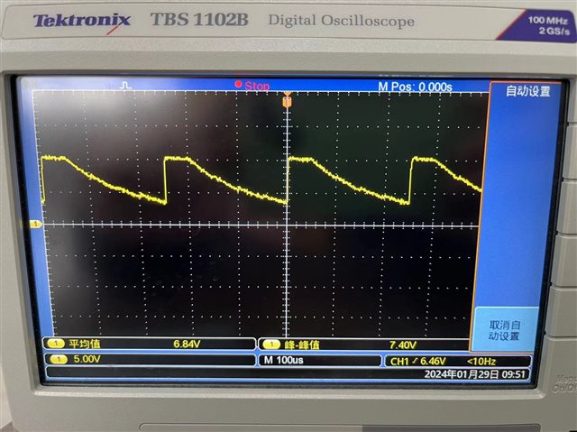
This looks like the charge pump is being overloaded. The maximum load is 10uA. Could you check that this is not being exceeded between the CHG and DSG FETs?
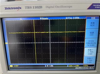
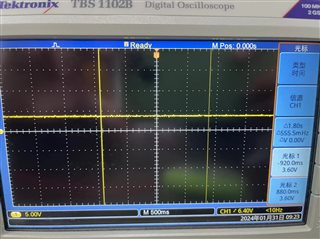
Also, just to double check the supply, could you capture the same waveform with the VDD and BAT voltages included?
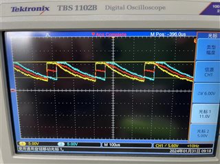
Hi Maxwell, Thank you TI two engineers to help! I checked the datasheet, the detection delay is 250us, it seems to trigger the Short circuit discharge, but I don't have a load connected to it, can you tell me specifically how to test the CHG and DSG FETs. Here are my VDD and BAT waveforms.
Looking at the waveform of CHG and DSG it looks like the charge pump is being overloaded when both outputs are being driven.
Are you able to try forcing either an OV or UV condition with a power supply to cause the device to stop attempting to drive one of the FETs and see if the other output becomes stable?
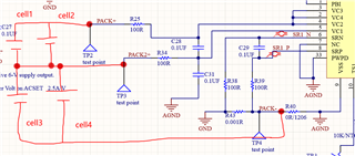
You may also try removing R62 and R66 and placing ammeters in their place to see what the current load on the charge pump is.
After I triggered OV and UV protection, it only closed the corresponding FET, but the other FET is still the waveform sent to you above, CHG pin and DSG pin, the ammeter shows 1uA.
Is the cause of this anomaly related to the selection of my resistance value? I hope you can help me confirm it.
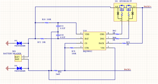
My design is built on the bq2980EVM as I understand it. Can you please provide a reference design about how the bq2980s are combined into a battery pack.
U6 is charging abnormally, discharging normally.
U7 is charging abnormally, discharging abnormally.
U10 and U11 are charging normally, discharging abnormally.
We don't have any reference designs as this device was not made with stacking in mind. This previous E2E thread (link) goes into more detail on the topic.
What do you mean when you say that the AFE is charging abnormally and discharging normally? Do you mean that the CHG pin is showing the abnormal waveform and the DSG pin is at a normal/stable voltage?
The BQ2980 isn't designed to be stacked. I don't think connecting the AFEs together after the protection FETs will work as if the FETs turn off on one device it could leave the ground reference floating on the upper device.
Also, there shouldn't be a need to have a separate AFE for each parallel cell. The parallel cells can be treated as a single cell since the voltages of each cell will equalize.
I recommend taking a look at the BQ77307. It is our new 2-7s protector and provides more integration than the BQ2980 and supports 2 cell systems. It may also be easier/cheaper to design in the BQ77307 rather than try to stack multiple BQ2980s.