This thread has been locked.

If you have a related question, please click the "Ask a related question" button in the top right corner. The newly created question will be automatically linked to this question.

UCC28070: UCC28070

Part Number: UCC28070
Other Parts Discussed in Thread: UCC27324-Q1, UCC27324

Hi TI Team,

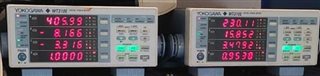
I am using UCC28070 for interleaved PFC, Power 3.5KW

while testing we loaded 3.3KW using rheostat load but Power factor remains at 0.95 only kindly advice me what components to be changed in schematics,i used Excel sheet and webench for design

Attached input and output values

Thank you

Venkatesh B

  • Hello Venkatesh, 

    If it is possible, please attach a PDF of your PFC schematic diagram, including values for the boost inductors.  

    Low PF can be due to input current phase shift and from harmonic distortion. 
    If you have a lot of X-capacitance in your line filter, displacement current in these capacitors can result in significant phase shift at high input voltage (230Vac), which reduces the PF.   
    If you have very low boost inductance, inductor switching currents may operate in DCM (instead of CCM) over much of the line cycle and that increases distortion which reduces PF.  

    For a temporary test, if you can remove some or all of your X-caps from the line filter, retest for PF at the same power level and see if PF has significantly improved. 
    If not much improvement, then you may conclude that most of the low PF comes from harmonic distortion.  Then investigate your inductor currents to see if they are working mostly in DCM or in CCM.  If mostly in DCM (and X-cap phase shift has been removed), then the boost inductance must be increased to work more in CCM. 
    A quick test of this is to temporarily wire in another inductor in series with the existing inductors, to double the inductance, then test PF again. 

    If it is already mostly CCM, then something in the current sense path may be adding distortion to the current signal.  It could be wrong Rsynth value (too high or too low), or current -sense transformers with too-low of magnetizing inductance or insufficient reset.

    Debug one step at a time, to eliminate each possibility in turn and converge on the root cause. 
    Don't try to change everything at once to save time, because you won't be able to correlate which change caused which result.    

    Regards,
    Ulrich

  • Hey Ulrich,what a nice debug method,i will try one by one and check,actually input side CMC & DMC also there,i will remove those too and check

    Thanks ulrich

  • Hi ulrich,

    I have done those methods and culprit is burden resistor, after changed those values with new one,now we achieved 0.96 at 800W and 0.99 at 2.4KW.Now problem is beyond 2.4KW one of the Mosfet blown away after some time , while observing thermal temperature gradually increases max 100 deg celcius

    kindly advice me to proceed further.

    I want very less ther1172.pfc.pdfmal dissipation also to keep it inside enclosure

    2nd problem is that output voltage (V=405V ) is started to decrease at 2.4KW

    Give suggestion to improve further

    Attached pdf of schematic as well

    Thank you

    venkatesh B

  • Hello Venkatesh, 

    Thank you for providing the schematic diagram of your board.
    There are some major issues with several component values and net connections. 
    Please verify that your board is constructed exactly as shown in the schematic, or if some part values are different on your board than shown in the schematic.
    If there are any differences in values or connections, please let me know what the differences are (or better yet, please resend the schematic with the corrections already made).

    Also, please provide this information: 
    Maximum PFC output power required.
    Min and max input voltages and line frequency ranges.
    Expected output voltage target.

    Your power meter reading (1st post above) shows 405V output, and your last posting indicates 405V, but the VSENSE resistor divider values on the schematic calculate to 391V for Vout.  That is one of the reasons why I ask if some part values on your test board are different than on the schematic. 
    I don't want to review a document that is different than the board that is being tested/debugged. 

    Boost inductors are shown as 110uH, 10A.  Are these ferrite-core inductors or powdered metal?  If a powder core, what is the 0A inductance, please?

    1. On the schematic, R221 and C231 are connected to the junction of R219 and R220.  This is incorrect. 
        Please connect R221 and C231 directly to the VINAC pin, on the right side of R220.  Leave R219 in series with R220. 
    2. The U28 VREF pin (pin 13) should have a 0.1uF filter capacitor to GND-P.
    3. Filter caps C227 and C229 on CSA and CSB are shown as 0.22uF each.  These values are much too high. 
        Please change C227 and C229 to 100pF each. 
    4. Value of C236 on CAOA should be 330pF, the same value as C234 on CAOB. 
    5. Soft-start capacitor C230 value should be >/= C220 on VAO; 1.5uF or higher.  
    6. R215 = 12kR on DMAX (pin 20) allows only 0.64 maximum duty cycle.  I suggest to increase to at least 0.94 => R215 = 37.4kR.
    7. I recommend to jumper CDR (pin 1) to VREF (pin 13) with a very short piece of wire, to disable frequency dithering during board debug.
        Dithering can be re-enabled and optimized later after your PFC is operating to satisfaction. 

    There are other issues that can be improved, but first I'd like to see responses to my questions and concerns above.

    Regards,
    Ulrich

  • Hi ulrich,

    I have done the changes.

    Now started to test using rheostat load.Regarding the choke 0A value is 260uH and at 16A ,65uH tested same using DCR test(magnetic vendor itself)

    Now Power=3500Watts,input is 230V AC output voltage is 410V DC,switching frequency fime tuned to 80KHZ

    Till 2.9KW output voltage maintains at 409V,beyond it voltage drops incrementally.

    Moreover one of the Mosfet and Diode reached 80 deg celcius still keep on increasing to avoid thermal failure we stopped at that point

    what could be the reason for this voltage dip and thermal heat at Mosfet and boost diode

    Kindly help me to solve this,attached the updated schematic

    pfc_80khz.pdf

    Thank you

    venkatesh B

  • Hello Venkatesh, 

    Thank you for the updated information and schematic diagram.  They are helpful.  I see that you have made many changes to the schematic.

    I cannot determine why Vout drops fro Pout > 2.9kW.  The converter may be power limited by the IMO resistance. 
    But Rimo is determined by full power at the lowest input voltage, and you indicate only 230Vac.  There has to be a +/- tolerance on that spec.
    Is it simply 230V +/-10%, or a wider range like 170Vac to 265Vac, or something like that?  

    The MOSFET and Diode heating is most likely a thermal-management problem, not an electrical one.  That is, there may be insufficient heatsinking for those components.  If the electrical design is all balanced, it is not likely that one phase dissipates more power than the other phase.   It is more likely that one side doesn't receive as much cooling as the other.  I suggest to analyze your airflow and cooling paths to see if the thermal impedances are equal or unequal. 

    Also, check to see if a hot component near the MOSFET/diode may be overheating them by proximity. 

    What is the real part number of the gate-driver IC?  You show an 8-pin part, but provide a part number for a 5-pin driver. 

    Regards,
    Ulrich

  • Hi Ulrich,

    Driver IC part number is UCC27324-Q1 , it is a 8 pin IC only and Input AC voltage range is 180V AC to 265V AC

    can i need to change IMO and RIMO value to optimize at full load?

    Kindly advice me

    Thank you 

    venkatesh B

  • Hello Venkatesh, 

    Thank you for the AC input information.  That is important. 
    I believe that several components need to be changed (including Rimo) to operate at full load.

    I have filled out the UCC28070 Excel Design tool with values that I think should work for you. 
    Starting with known information and a target Pout = 3316W (same as on the power meter at the top of this post), I estimated the design as I think you are targeting.  I included a +10% margin for input current that is not reflected in the Pout target, but I included it in the Rs and Rimo values.
    Several component values I kept the same as in your latest schematic diagram, but many others I recommend to you to change as indicated in this file: 
    UCC28070 Design 3.3kW (VB).xls
    Note: Some of the values I entered are different than what the tool recommends, and this is intentional because I am accounting for very high ripple current that the tool does not handle effectively.

    Also please note:  Your inductor design has widely varying inductance with current (this is known as a "swinging choke") and leads to 18.4A pk-pk ripple current at full load (PFC 3316W out), 180Vac input.  This ripple will appear superimposed on the average peak current of 14Apk in each boost inductor.  So peak inductor current will be 14A + 18.4A/2 = 23.2Apk in the inductor.  And even higher (~24.6Apk) during transient load steps when the extra 10% capability is used to restore Vout regulation.  

    The issue is that the inductor data provide characterized boost inductance (Lb) as 65uH at 16A, but current up to 24.6Apk will reduce Lb much more.
    However, my 18.4Apk-pk calculation is made from 65uH, no the lower Lb as current increases > 16A.  So the actual peak is probably much higher, and can lead to peak-limit issues or other problems.  Since the "soft-saturation" of a swinging choke is non-linear, it is very difficult to predict the final inductance and final peak current without a characterization curve of Lb vs. Idc for Idc > 25A, maybe up to 30~35Adc.  

    Is it possible to redesign the inductor for less swing, to keep the ripple current under control? 

    Other comments:
    1.  You show SiC MOSFETs rated at 900V for boost switches at a ~410V output application.  This seems excessive and 650V Fets are available from Wolfspeed which can have lower Rds(on) and maybe less expensive.
    2.   I suggest to consider SiC diodes for the boost outputs to avoid reverse recovery currents from the existing fast-recovery Si diodes.  As the Si diode heat up, their Irr gets worse and switching losses will increase.  SiC diodes may have a little higher Vf, but have no Irr, and lower Cj.   At fSW = 80kHz, I think this could be a net reduction in losses.     
    3.  Inrush bypass diode D50 does not need to be an ultrafast recovery diode.  A standard recovery diode is okay for this application.  And it does not have to be rated for 20A average.  It should be rated to carry the peak inrush current.  Inrush limiting is not shown on your schematic, but diodes smaller than 20A avg still can have relatively high peak surge capability and be less expensive.
    4.  The SiC MOSFETs are optimized for +15V on and -4V off gate drive.  The UCC27324 driver can provide only ~12V on and 0V off drive.  Since the SiC Fets have a threshold voltage about ~2V, make sure your gate-drive path is very short with negligible inductance to avoid noise and other effects causing unwanted turn-on of the Fets.  Also make sure that the Rds(on) value that you use for loss calculations is adjusted for the lower Vgs and for increased Tj. 

    Regards,
    Ulrich

  • Hi ulrich,

    Thank you for the calculation,i have done as per your calculation(little change) and tested with little changes in Heatsink and Diode replacement,Now its working well and good and temperature is stable at 70 dec celcius

    1.All components changed with respect to calculation,i edited one value in that excel sheet Current transformer(200:1 from 100:1)

    2.PFC diode changed to SIC diode(Before it was Ultrafast rectifier)

    3.Heatsink of PFC diode is doubled and all diodes at same heatsinK(Earlier different individual heatsink)

    I have requested magnetic vendor to give less swing L value, will update in next version

    Thank you so much for the timely support

    only one doubt input side AC voltage is reduced to 209V at full load(3.2KW) from 230V AC when no load is connected,is there any way to improve this line regulation

    Note: I am using Variac

    Thank you

    venkatesh B

  • Hello Venkatesh, 

    I am glad that the PFC is working better for you now and I hope a lower swing (inductor) will help even further. 

    As for the voltage drop from the AC Variac, that is a function of the impedance of the Variac.  The drops are due to resistance and leakage inductance.
    The only remedy is to get a bigger Variac (which will reduce but not eliminate the V-drop), or procure (buy or rent) a 5-kW programmable AC source.

    With the Variac, if the output voltage does drop from 230Vac at no-load, you can manually dial it up higher again to compensate for the voltage loss under load. An electronic AC source will regulate its output to the set point, so no adjustment should be necessary as the load varies.

    Regards,
    Ulrich 

  • Thank you ulrich,i will try it.

    I hope if we connect to Grid direct 230V line regulation will be good

    Thank you