- Ask a related questionWhat is a related question?A related question is a question created from another question. When the related question is created, it will be automatically linked to the original question.
Original question:

Tool/software:
Hello!
I am currently experimenting with an SMPS based on the "400- to 690-V AC Input 50-W Flyback Isolated Power Supply Reference Design for Motor Drives."
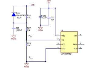
Contrary to the guide, I am not using a cascade connection at the moment. I am using a single MOSFET as shown in the diagram, and the MOSFET is the same as the one selected in the guide.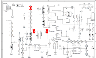
Currently, only the initial 3 PWM pulses are being output, and the system is not operating properly. Therefore, I measured the VS and CS pins.
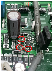
To minimize risks during measurements, I kept the lead wires short. My experimental setup is as follows:Red circle are lead cable using measurement.
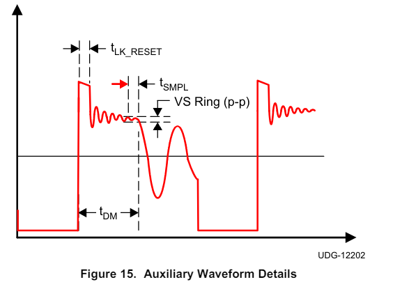
For the CS pin voltage: It is in a no-load condition with a shunt resistor of 1.2 ohms. I observed the following waveform. I think this voltage spike is caused by the measurement cable. Therefore, I believe it has not reached the protection voltage. Could you provide any comments on this?
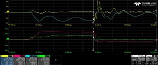 (CH1: Vcs, CH2: VDS, CH3: Vaux, CH4:Vgs//Test input voltage : 500Vdc)
For the VS pin voltage: It is also in a no-load condition, and the waveform is as follows. I think the current voltage on the VS pin is higher than the operating level. So, I am considering reducing the value of R_vs. Could you provide any opinions on this?
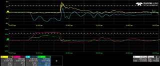 (CH1: Vvs, CH2: VDS, CH3: Vaux, CH4:Vgs//Test input voltage : 500Vdc)