TPS63021: Converter does not switch from PS to PWM mode

Part Number: TPS63021

Tool/software:

Hey

In the Null-Series production, we discovered in the PCBA componente test that not all the TPS63021 DC/DC converters behave the same regarding the Power-Save Mode. We can identify two clusters of devices, where 3/4 of them switch between the power save and PWM mode as expected (Cluster 1) and 1/4 remain in the power save mode (Cluster 2). The PCBA componente test stimulates a load current >350mA on the 3.3V domain, supplied from the TPS63021, with a static 9Ohm load. All the prototype deveices we produced before behave as expected and switch at approximately 100mA from PowerSave Mode to PWM Mode. Therefore, we first searched for an issue in the assembly of the board. But in the end it came down to the TPS63021 itselfe, which makes the differnce. Besid the voltage level also the input current repective the efficency is differnt between the two clusters.

Cluster 1 :
* TPS Vout: 3.28-3.30V
* Input Current: 372 - 380mA

Cluster 2:
* TPS Vout: 3.38 - 3.46
* Input Current: 405-420mA

Two interesting observations:

* If the device is fully assembed with a CPU module supplied from the 3.3V domain, which causes a similar load current as the test load but with load transients smaller and bigger. All the TPS switch to PWM mode.

* If the PCBs from cluster 2 are modified, so that the TPS is forced to PWM Mode (PS/SYNC pin high) and tested again, Vout and Input Current are equal to the cluster 1 boards.

I did not measure the inductor current but assuming the average inductor current corolates with the output (load current), I would expect that according to the data sheet a switching from PS to PMW mode happens at around 100mA load current.

We implemented the DC/DC converter prety much according the reference desing from chapter 8.1 in the data sheet.


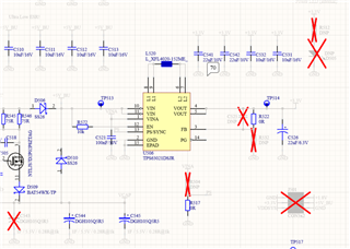
Now is the question whay do we have observe this two clusters regadeing the 3.3V supply domain. Do we have a misunderstanding of the Power Save mode control of the DC/DC converter, is there a inssue with the TPS63021 devices we sourced for series production or anything else?

Did anybody do similar observations with the PC/PWM switching behaviour of the TPS63021 or has an explonation for the above described behaviour?

Thank you for your respons and help.

  Simon

  • Hi  Simon,

    I am confused about your description. Both cluster1 and cluster 2 has 350mA higher input current, and both of them work in PWM mode, is it not expected?

    For TPS63021, threshold for PSM and PWM mode transition is current of inductor close to 100mA. 

    Regards

    Tao

  • Hey Tao
    The PCBA under test is a carrier board (or mainboard) for a pluggable CPU module. This mainboard is equipped with peripherals like GPS module, supervisor MCU, and the like, also supplied from 3.3V domain. But those components drew less than 100mA.
    While testing the mainboard PCBA with a needle adapter in the production line the main load on the 3.3V supply, the CPU module, is not assembled at this stage. To simulate the CPU module load, we apply a 9 Ohm resistor to the 3.3V voltage domain.

    With that 9 Ohm resistor load, the load current on the TPS63021 is similar to the device's normal operation with the CPU module running and clearly above the PSM/PWM transition threshold.

    In that configuration, we expect to see on all boards the TPS63021 running in the PWM mode. However, some of them remain in PSM mode (cluster 2). This leads to a 3.3V supply domain voltage level of ~3.4V and a bad efficiency with a ~30mA higher input current.

    We do not understand why the TPS63021 on some boards does not do the transition from PSM to PWM mode, although the load current is clearly above 100mA. This behavior is stable and reproducible. If we force the conspicuous TPS63021s that remain in PSM mode to high by pulling the PS/SYNC pin. The converters work as expected and the Vout voltage and efficiency are in the expected range.

    But we would like to take advantage of the power-saving feature of the TPS because we have low power operation mode of the device where almost everything except the MCU is disabled, to "sleep" as long as possible from a backup energy storage.

  • Hi  Simon,

    Got it, thanks for your explanation.

    So far,  we just speculated based on the output voltage, input current and some comparative experiments that some device from cluster 2# are working in PFM mode, right? Mostly, i agree with you but it is better if you can help to confirm by waveform of switching node or current of inductor.

    From my side, i will check internal about the distribution of threshold between devices(100mA averange inductor current)

    Regards

    Tao