LM5176: Output Overvoltage Protection (OVP) activates as soon as input voltage reaches above 35V

Part Number: LM5176
Other Parts Discussed in Thread: LM5177

Tool/software:

Dear all,


I'm designing a buck-boost converter using the LM5176. The input voltage ranges from 21V till 54V. The output voltage should be 24V (fixed). The maximum output current is 9.2A.


The converter seems to work fine when the input voltage is below 35V. However, when the input voltage reaches above 35V, the output voltage rises to about 26.5V and then the Output Overvoltage Protection (OVP) activates. As soon as the OVP activates, the voltage drops. When the voltage is low enough (when the OVP disactivates), the converter starts up again, and the steps above are repeated.


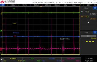
I have tried to capture some useful information. Please find some oscilloscope screenshots below.


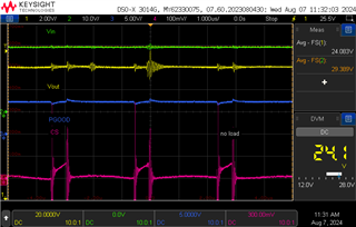
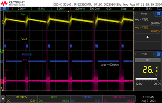
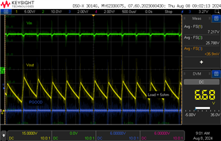
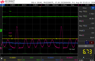
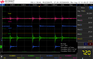
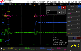
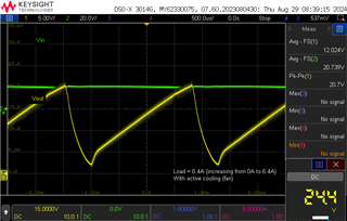
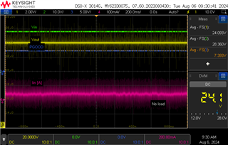
This first screenshot shows operation at an input voltage of 28V (green trace). The output voltage is 24V (as needed) (yellow trace). The PGOOD pin is pulled high (indicating that everything is fine) (blue trace). The input current is constantly about 20mA (pink trace). As explained above, the converter seems to work fine when the input voltage is below 35V (as shown in this screenshot).


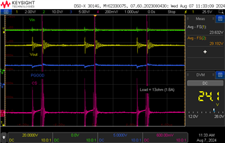
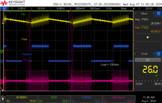
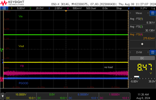
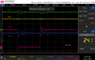
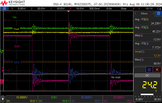
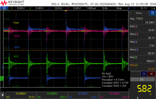
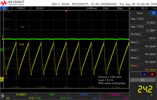
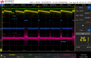
The second screenshot shows operation at an input voltage of 36V (green trace). The output voltage constantly switches between approximately 26.5V and 25.8V (yellow trace). The blue trace shows that the PGOOD pin indicates that converter only sometimes works fine. The pink trace indicates that the input current drops to 0A when the PGOOD pin is not high (indicating that the converter turned off due to OVP).


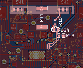
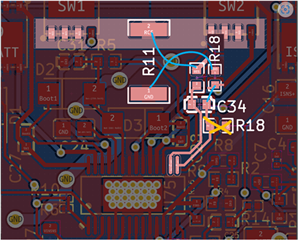
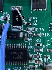
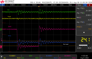
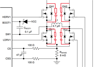
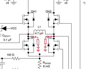
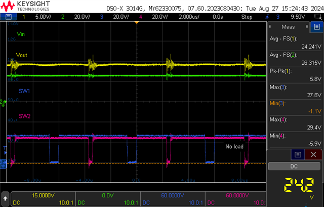
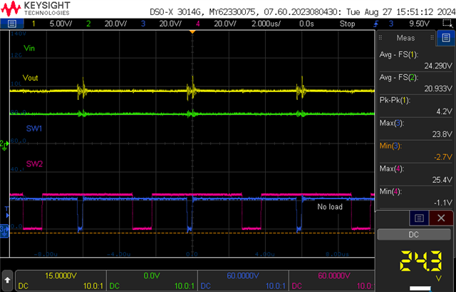
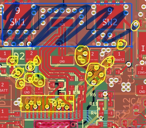
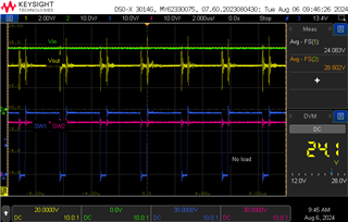
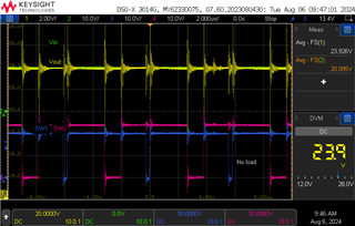
I also took two screenshots of SW1 and SW2 (the first one at buck-boost mode and the second one at buck mode). I’m not sure if this information is helpful for this problem.


Finally, I also took a video in which I increased the input voltage. You can see that at about 35V input voltage, the controller’s OVP activates.

Click here to play this video

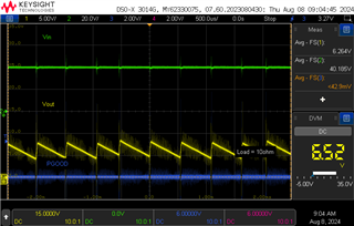
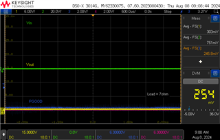
Please be aware that all tests and screenshots above, are without any load.

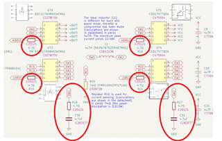
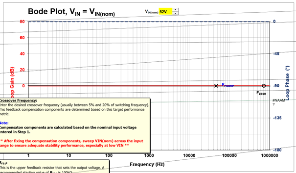
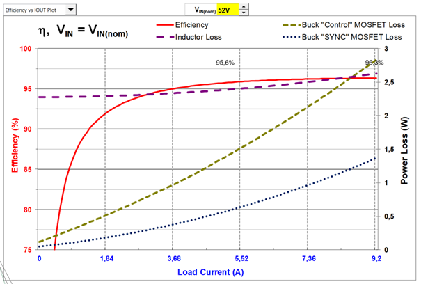
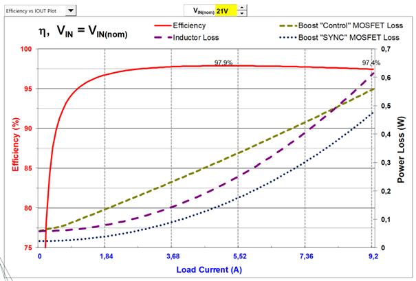
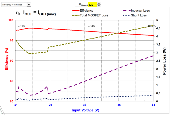
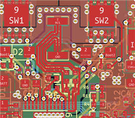
I designed my schematic using WEBENCH. This is the schematic:

2577.Schematic.pdf

I'm looking forward to your reply!

Best regards,

Max

  • HI Max,

    how is the behavior then with load?
    Is this only on one board or have you more with the same behavior?

    Can we also review the layout - esp. the CS current sensor connection - has this been done as a Kelvin connection?

    Best regards,

     Stefan

  • Hi Stefan,


    Thanks for your quick reply!


    When the input voltage is less than 35V and the load is less than 2.5A, everything works fine. When the input voltage is less than 35V and the load is more than 2.5A, the controller shuts down (this is not expected since the controller should handle 9.2A). When the input voltage is more than 35V and a load is connected, the controller still doesn’t work (it shows the same behavior as without load).


    I have got five of the exact same PCBs. Currently, I tested two PCBs and they both show the exact same behavior.


    I took a screenshot of the CS current sensor connection layout, please take a look below. Resistor R11 is the current sensing resistor and R15, C34 and R18 create the RC filter network. As you can see, I did not take a Kelvin connection into account.


    I performed some measurements at the CS/CSG pin (I used a probe ground spring).

    The first screenshot/measurement shows the controller with an input voltage of 29V and no load. Everything seems to work fine.


    The second screenshot/measurement shows the controller with an input voltage of 29V and a load of 13ohm. Everything seems to work fine.


    The third screenshot shows the controller with an input voltage of 29V and a load of 9ohm. The load seems to draw too much current, which causes the controller to shut down.


    The fourth screenshot shows the controller with an input voltage of 41V and a load of 500ohm. The controller still shuts down due to the OVP.


    The fifth screenshot shows the controller with an input voltage of 41V and a load of 100ohm. The controller still shuts down due to the OVP.


    Please let me know if you need more information/measurements.

  • HI Max,

    thanks for the additional info.

    I assume that the current sense signals is heavily interfered with signals coupled in and might also see an ground shift as this also has different connection points to the GND layer.

    The CS signals is also connected to the MOSFET and not the R_CS where an additional shift and distortion can be generated.

    Note: The CS signal is the most important control signal for this controller and needs to deliver a proper signal.

    You might try to update the PCB with some blue wires to get a more optimized routing. If so please use twisted short wires only.

    Best regards,

     Stefan

  • Hi Stefan,


    Thanks again for the quick reply!


    I have updated the PCB as you suggested, please refer to the photo below (the blue cable can be ignored, because it is just to easily connect a probe to the PGOOD signal). Now, the current sensing resistor is connected using the Kelvin method.


    This PCB modification fixed the problem that the system didn’t work at input voltage higher than 35V. So, the PCB now works at any input voltage range of 21V till 54V without load.


    After discovering that the PCB works fine without load, I started testing with load at different input voltages.

    Firstly, I started testing at an input voltage of 26V. I found out that the PCB works fine with loads higher than 6ohm. However, as soon as the load decreases to 5ohm, the output voltage drops to about 7V (and a saw waveform is created). At loads of 5ohm (or lower), the PGOOD signal indicated that the controller wasn’t working properly. Please refer to the screenshot below.


    Secondly, I continued testing with a higher input voltage of 40V. FYI: The PCB was not (permanently) damaged by the behavior as described above. I found out that the PCB works fine with loads higher than 11ohm. However, as soon as the load decreases to 10ohm, the output voltage drops to about 7V (and a saw waveform is created). At loads of 10ohm (or lower), the PGOOD signal indicated that the controller wasn’t working properly. As you probably have noticed, this is the exact same behavior as described above. Please refer to the screenshot below.


    Have you got any idea why a saw waveform is created when the load draws too much current?


    Thirdly, I continued testing with a higher input voltage of 52V. FYI: The PCB was not (permanently) damaged by the behavior as described above. I found out that the PCB works fine with loads higher than 8ohm. However, as soon as the load decreased to 7ohm, the output voltage dropped close to 0V and the input voltage dropped as well. I then noticed that the power supply that I was using, was shorted. The PCB is now permanently damaged, it keeps acting like a short (also at lower input voltages). The screenshot below shows that the PCB is not working.


    I found out that, after removing MOSFETs U70 and U72 (those are the MOSFETs connected to HDRV1 and LDRV2), the short is gone. So, it seems like MOSFETs U70 and U72 couldn’t handle the high current in combination with the high voltage. FYI: MOSFETs U70 and U72 are the BSC117N08NS5ATMA1.

    Do you think that MOSFETs with higher voltage and current ratings should fix this problem?


    Looking forward hearing from you!

  • I just faced a new issue with a new PCB. I was testing a new PCB, to see if its behavior is the same as the previous one.


    The new PCB worked fine for a few minutes. I slowly increased the input voltage from 21V to 52V. I let the PCB work at 52V input voltage for a few minutes, and then suddenly the output voltage dropped to about 8.5V. Now, it keeps outputting 8.5V (instead of 24V), also at lower input voltages. Please take a look at the screenshot below.


    FYI: I also updated this new PCB with the Kelvin connection of the current sensing resistor, so that did, probably, not cause this new issue.

  • Hi Max,

    can you first check VCC on the broken board - is this still 7V?

    If not you may have large under of overshoots on the SWx nodes (which you should anyhow check).

    If this is the case this can easily damage the device and need to be filtered by e.g. snubbers and or gate resistors.

    Best regards,

     Stefan

  • Hi Stefan,

    Thanks again for your help! That's great because I'm a student with very little experience with DC-DC converters.

    That's a good idea to check.

    Just to be sure: should I check the VCC (and SWx nodes) of the broken PCB that now outputs 8.5V instead of 24V (or the one with the short, described two messages above)?

    When is the under-/overshoot (of the SWx nodes) too large? I already noticed some over- and undershoot, but I have no idea what is normal/typical (I'm not in the office at the moment, I will share a screenshot of the over-/undershoot tomorrow).

    And one more question (sorry for the many questions, I hope it's not too much): Do you recommend a specific resistor value to be placed in series with the gate?

  • HI Max,

    when I say VCC - i mean the VCC pin of the LM5176

    I just assume that one of the output drivers got damage due to electrical overstress. Often this leads to and higher load of the LM5176 VCC so that it does not reach its target level of ~ 7V.

    Esp. with higher input voltage the under or overshoot on SWx can happen which leads to the overstress.

    See also:

    https://www.ti.com/lit/ta/ssztbc7/ssztbc7.pdf

    https://www.ti.com/lit/an/slyt465/slyt465.pdf

    For the allowed over and undershoot please check the abs max ratings:

    Note: when using gate resistors, this should be less then 5Ohm for this devcie.

    Best regards,

     Stefan

  • Hi Stefan,


    The VCC of the broken PCB (that outputs 8.5V instead of 24V) indeed doesn’t reach 7V. So, that must mean that electrical overstress is occurring. The SWx node’s voltages also look quite strange, but that’s probably due to the overstress.


    I performed measurements on a new PCB (which is, of course, working properly). It turns out that there is quite some ringing on the SWx nodes. The absolute maximum ratings of the SWx nodes are already violated, at an input voltage of 30V.


    The ringing can also be seen at the VCC node.


    At even higher input voltages, the ringing gets bigger and the SWx node’s voltage rises, which violates the absolute maximum ratings of the SWx nodes even more. The ringing can be seen even more at the VCC node.


    After this discovery, I tried to implement a RC snubber on the new PCB. Is used this https://www.ti.com/lit/ta/ssztbc7/ssztbc7.pdf document to find the correct snubber resistor and capacitor. Ater the measurements/calculations, I found out that the snubber resistor should be 35ohm and the snubber capacitor should be 444pF. I used a 33ohm resistor and a 300pF capacitor. I soldered the snubber circuits as shown below:

    However, it seems like the snubber circuits do not affect the over-/undershoot. And in the meantime, the new PCB with the snubber circuits (that was working fine) is also broken and outputs a very low voltage as well. I now only have one brand new PCB. So, could you please verify if the snubber circuits are right (before I’m going to modify the last new PCB)?

  • Hi Max,

    a resistor of 33 Ohm sounds to large for a snubber. I would more expect in the range of 3.3 Ohm.

    A snubber is only required on SW1 and SW2 and can be to GND

    Or you can place them on QL1 and QH2

    Best regards,

     Stefan

  • Hi Stefan,


    Thanks for the clarification!


    I decreased the resistor to 4.7ohm and I tried several capacitors (ranging from 1nF to 10nF). I also changed the connection of the snubber circuits, now I only have two snubber circuits which are connected to SW1/SW2 and GND (as shown below).


    It seems like I get the best result when the capacitor of SW1 equals 4.7nF and the capacitor of SW2 equals 2nF. At Vin = 35V, I get the following:


    At Vin = 50V, I get the following:


    The snubber circuits definitely decrease the over-/undershoot. However, it seems like the over-/undershoot is still too big. And a much larger snubber capacitor seems to effect the square wave (the signal is completely modifed than).


    It is very hard to add a series resistor (of max. 50ohm) in series with the gates on this PCB. So, I cannot test if a series resistor decreases the over-/undershoot enough.


    Have you got any advice?


    PS I have a lot of screenshots (like the ones above) at different snubber capacitor values, but I’m not sure if that’s needed for you.


    Best regards,

    Max

  • Hi Max,

    just to ensure Rgate should be less then 5 Ohm  (you wrote 50 Ohms above) !

    When measuring the SW signals please ensure a proper probing. You need to minimize the ground loop - the standard ground clip of a scope probe is far to long and you pick up a lot of disturbances - best is a Tipp and Barrel setup.

    (+) How to measure ripple for better design outcomes - Power management - Technical articles - TI E2E support forums

    Common Mistakes in DC/DC Converters and How to Fix ...

    -> shows Tip&Barrell - page 28

    Best regards,

     Stefan

  • Hi Stefan,


    The soldered-on components are also creating quite big loops, which also don’t help. I think that I’m going to order a new PCB with 4.7ohm gate resistors, two snubber circuits (connected to SW1/SW2 and GND) and with Kelvin connections for the CS resistor and the ISNS resistor. Besides that, I have also re-routed some connections of the PCB to create a better design. I hope that this new PCB eliminates the downsides of the soldered-on components (which might worsen the performance). Have you got any recommendations before I order a new PCB?


  • Hi Stefan,

    Thanks for the tips! I took the tips into account, and I ordered the new version of the PCB. I will keep you updated how the new PCB functions (but this will not be in the next few weeks, since it takes over two weeks before the PCB gets delivered).

    Best regards,

    Max

  • Hi Stefan,


    The new version of the PCB has arrived. I was testing and everything works fine when the load is not bigger than 5A.


    I have made a screenshot of SW1 and SW2, just to be sure that the snubber circuits work as intended. I have used a probe spring for this measurement, however, I was not able to hold two probe springs at the same time (that’s why SW1 looks better on the first screenshot and SW2 looks better on the second screenshot).


    VCC also looks quite stable (minimum is 6.88V and maximum is 7.93V). So, I assume that the snubber circuits work like expected.


    When the load is quite a bit larger than 5A and I let the system run for a minute, the MOSFETs breaks down (shorting the input). I now have one PCB with a short after running for multiple minutes at 5.5A and one PCB with a short after running for about half a minute at 9.5A. Have you got any recommendations? Should I replace the MOSFETs to check if only the MOSFETs are damaged and the chip itself still works?


    Best regards,

    Max

  • HI Max,

    If the MOSFET got damaged due to thermal overstress, then typically only the MOSFET is damaged.

    If VCC on the damage boards are still OK then there is a good chance that only the MOSFET is damaged.

    Next you can remove the damaged MOSFET and check if VCC is still OK then there is a good chance that only the MOSFET is damaged.

    Otherwise replace the LM5176 as well.

    Did you observe the temperature of the MOSFETs while increasing the load - was the temperature still in the expected range?

    Best regards,

     Stefan

  • Hi Stefan,


    Once again, thanks for the very quick reply!


    I removed MOSFET HDRV1 and LDRV2 on both damaged PCBs (those are the only two MOSFETs that were damaged). After removing those two MOSFETs, I measured the VCC. The VCC seems ok at both PCBs (VCC was about 7V). So, I assume that thermal overstress (of the MOSFETs) caused the damage.

    After this discovery, I replaced both MOSFETs (with new ones). It turned out that both PCBs work fine after this replacement. So, only the two MOSFETs were damaged.


    Is it normal/typical that those two MOSFETs experience the most heating?


    I assume that I should just place extra MOSFET(s) in parallel, to reduce heating, right?


    Unfortunately, I did not observe the temperature of the MOSFETs while increasing the load. I will monitor the temperature from now on. I already discovered that the MOSFETs reach about 45 degC when there is no load connected. Is this normal/typical?


    Best regards,

    Max

  • Hi Max,

    yes, this are the MOSFETs which typically have the highest losses.

    To find out if this is expected or not you would need to calculate the losses in the MOSFET and check it with the Thermal parameter from the datasheet.

    The quickstart calculator or the application section in the datasheet can help you on that.

    Best regards,

     Stefan

  • Hi Stefan,


    I’m currently testing with active cooling (a fan) and the PCB can already supply 6.4A (for over 2 hours)! So, it really seems like an overheating problem.


    I assumed that you mean the Excel sheet (https://www.ti.com/tool/download/SNVC208) by the “quickstart calculator”. I have filled in this Excel sheet, however I didn’t knew what to fill in at “Desired Crossover Frequency”. I also noticed that at “Step 7: Compensation Design”, some information is not filled in, please take a look at the screenshot below (looks like an Excel error).

    The bode plot is also not filled in.


    I don’t think that the errors above matter for the overheating calculation for the MOSFETs. That’s why I just continued to fill in all information about the MOSFETs. I get the following plots:


    I assume that I should use the power dissipation of the MOSFETs and compare it to its datasheet. However, I’m not quite sure how I should do this (which exact params should I compare?).

    5466.LM5176 Buck-Boost Quickstart Tool.xlsm

  • Hi Max,

    something in the excel sheet was corrupted, so i copied the data to a new one - attached.

    5466.LM5176 Buck-Boost Quickstart Tool (1).xlsm

    The the mayor issue would be from the losses of the BUCK side MOSFET 

    The chart shows here a loss of  almost 3W - if the Theta JA value in the Excel is correct (20Deg/W) sounds very low.

    then the temp would increase by 60 Degree. Typically this value is more in the range of 50 which would lead to 150 Degree.

    Best regards,

     Stefan

  • Hi Stefan,


    Thanks for fixing the Excel document! Then it would make sense that the MOSFETs break down at high output currents. I will just add extra MOSFETs in parallel (and add active cooling (fan)).


    I have noticed one more issue (hopefully the last issue ;) ). At high input voltages (31V till 54V) the system can reach the desired output current of 9.2A (as expected). At high input voltages (31V till 54V) the system can also handle large load transients (from 0A to 9.2A) (as expected). However, at voltages below 31V, the system cannot reach the maximum output current of 9.2A (not as expected). At low voltages (below 31V) the system can reach a maximum output current of 6.4A when slowly increasing the load. At low voltages (below 31V) the system cannot handle a load transient of 0A to 6.4A (the maximum load transient that the system can handle at low voltages is 0A to 4.7A). So, in summary: the system works fine at input voltages of 31V and higher, but at input voltages of 31V and lower, the system fails to handle high output currents.


    The screenshot below shows the output voltage of the system at a low input voltage (below 31V) and high output current. As you can see, the system constantly tries to startup, but it fails starting up.


    I already read that this might has to do with soft start capacitor (e2e.ti.com/.../lm5176-q1-lm5176-q1-full-load-start-up-at-lower-vin. I have increased (and decreased) the soft start capacitor, but this didn’t solve the problem.

    Have you got any idea what could cause this problem (and how to solve it)?

  • Hi Max,

    for me it looks like the current sense resistor is to large and you get over current events triggered.

    Suggest to change the Sense Resistor to  5.5 - 5.0 mOhm.

    Best regards,

     Stefan

  • I will check that.

    Do you mean the cycle-by-cycle current sense resistor (connected to the MOSFETs) or the average current sense resistor (in series with the output)?

  • HI Max,

    i mean the cycle-by-cycle current sense resistor (connected to the MOSFETs) connected to CS/CSG

    Best regards,

     Stefan

  • Hi Stefan,


    Lowering the sense resistor solved the issue for input voltages between 22V and 31V. I added a 7mΩ resistor in parallel with the original resistor of 7mΩ (resulting in a 3.5mΩ resistor). Everything now works fine for voltages above 22V.


    When the input voltage is between 21V and 22V, the system still doesn’t work when the load is more than 6A (please take a look at the screenshot below).


    Does this also has to do with the sense resistor or could something else cause this?

  • Hi Max,

    peak inductor current here is 12.2 A - what is the saturation current of the inductor you have used.

    Based on the excel calculator the slope compensation is also slightly higher then recommended (C value is lower then recommended)

    I do not think that this is the issue here but might be good to adjust.

    The sense resistor should be OK as the limit for over current detection is 100mA there should be enough margin, unless you have some issue with the layout of the sense resistor and pick up to much noise.

    Best regards,

     Stefan

  • Hi Stefan,


    The saturation current of the inductor is 41A, so that should be enough.


    I have increased the slope compensation capacitor to 680pF (because that is what the Excel document recommends at a 3mΩ cycle-by-cycle current sense resistor). I actually do not see any difference after this adjustment. Nevertheless, I will use a 680pF from now on.


    I’m having a really hard time measuring the cycle-by-cycle current sense resistor, because it seems like my probe influences the system (I already have my probe set to 10:1). So, it’s really hard to look for noise on this signal.

    I also tried to lower the cycle-by-cycle current sense resistor to 1.75mΩ (to allow even more current), but this resulted in the exact same behavior.

    This is the layout of the sense signal that I use:


    The layers are stacked as followed:


    The sense signals are connected by a Kelvin connection. I have added a not-connected trace (as much as possible) around the sense signals, to pick up any noise (and prevent noise in the sense signals). I have also placed a ground plane (which is only connected (to the other grounds) at one point) directly underneath the sense signals, again to pick up any noise (and prevent noise in the sense signals). Unfortunately, I somehow had to route the high di/dt and high dv/dt signals of the boost-leg underneath the sense signals (I used the orange layer for these signals).

    What do you think about this layout?


    Best regards, Max

  • HI Max,

    the layout looks good from the routing but you have used thermals.

    This could get critical for this amount of power you would like to have. Esp. for all components in the power stage this should be avoided as it adds inductance and increases the resistance.

    When measuring the sense resistor (this is not easy) you need to make the probe connection as short as possible.

    Using a tip and barrel is the best:

    Common Mistakes in DC/DC Converters and How to Fix ...

    -> shows Tip&Barrell - page 28

    Best regards,

     Stefan 

  • Hi Stefan,

    What do you mean by “thermals”? I’ not familiar with that term.

    Best regards, Max

  • Hi Max,

    Sorry for the confusion with the shorted phrase.

    Try to search in the internet for "thermal relief", you should then find the right information.

    Best regards,

     Stefan

  • Hi Stefan,

    Thanks for the clarification!

    I have used thermal reliefs at roughly three places, which I have marked in the screenshot below (blue at the top, yellow in the middle and purple at the bottom).

    Just to be sure: At which place(s) should I remove the thermal reliefs?

  • Hi Mason,

    not easy to see in the drawing above:

    so for sure the blue area, plus the GND side of the shunt

    I also would not use them then the middle layer.

    In general all paths where high dI/dt or dV/dt is there:

    - whole power stage

    - gate lines

    - VCC cap to LM5177

    Best regards,

     Stefan

  • Hi Stefan,

    Ok, thanks again for the clarification!

    One last question before I create a redesign: Is it ok to use thermal reliefs to route the sense lines (of the cycle-by-cycle current sense resistor) at the copper bottom? Because somehow the sense lines (of the cycle-by-cycle current sense resistor) need to cross the gate lines of the boost-leg, forcing me to place one of those lines at the copper bottom (and I need thermal reliefs to route a line from the copper top to the bottom).

    Best regards, Max

  • Hi Max,

    it is OK for the sense lines from the sense resistor to the LM5177 but not for the sense resistor.

    Best regards,

     Stefan

  • Ok, thanks! I will update the design