This thread has been locked.
If you have a related question, please click the "Ask a related question" button in the top right corner. The newly created question will be automatically linked to this question.
Dear community,
I would like to ask you for some help with my problem. I have designed circuit with LM46002 according to relevant datasheet. At first look at real board everything looks OK, Vout=3.3V, teperature is low. But when convertor works in load (300 mA), you can hear slight whistling from inductor and osciloscope image shows about 6 kHz ripple with 50 mVp-p, instead of expecting 500kHz what you can see in simulation.
Could this issue be caused by wrong Cff (phase margin capacitor)?
Schematic:
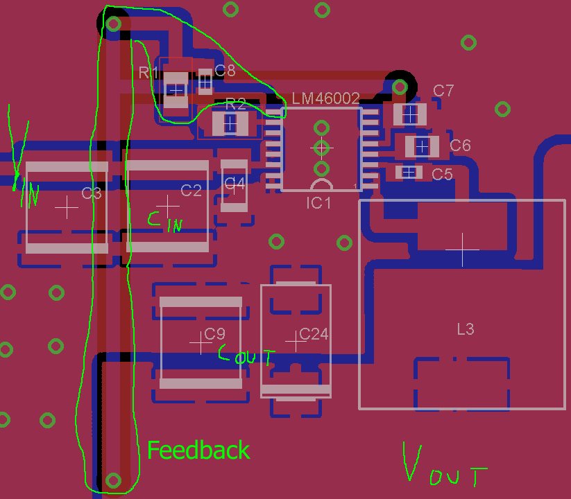
Layout:
Thanks.
What is your input voltage ?
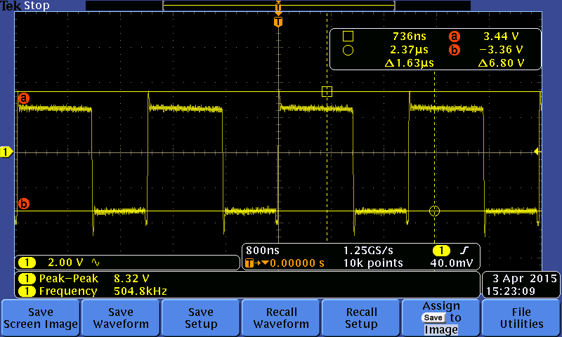
Can you show us the waveform on the switch node ?
The device may be in PFM mode.
Hi, the schematic and layout look ok. The only concern on the layout is that the traces to the SW pins and VIN pins are pretty thin. Wider traces reduce parasitic resistance and inductance.
For the oscillation at 5.97V input and 3.3V output, 300mA load, do you observe the same oscillation at other load or other Vin? Please probe VIN signal on the Cin caps when you observe the oscillation on Vout. Vin might be oscillation as well.
For the Cff value, it relates to the ESR value of the Couts. Could you specify the ESRs of the two output capacitors? If ESR is large on the Cout, please reduce Cff.
Also, you can reduce L to 10uH to increase peak to peak ripple on the inductor current, thus higher signal to noise ratio for the control loop.
Hope it helps.
Yang