This thread has been locked.
If you have a related question, please click the "Ask a related question" button in the top right corner. The newly created question will be automatically linked to this question.
Hi forum,
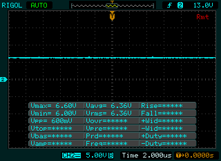
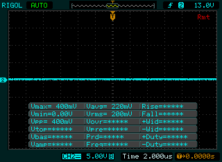
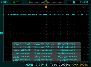
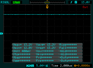
Im using the BQ24650 charge controller to charge VRLA.
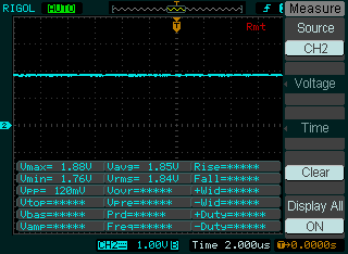
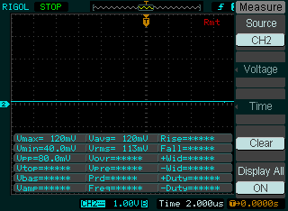
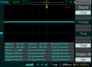
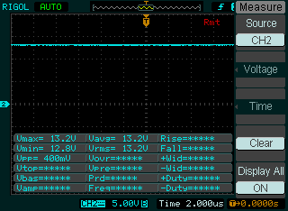
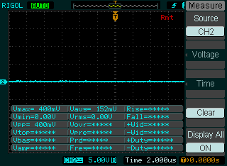
In my design process, I remove D2 and started a charge cycle.
The circuit, because it didn't had the High side driver, didn't start the charge process. (Correct me if i'm wrong)
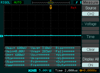
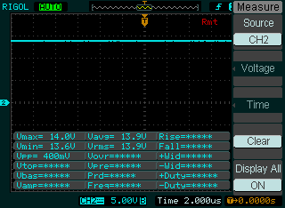
When I solder again D2 into the PCB, the circuit still didn't start the charge process.
My questions are:
Thanks!
Hi Jose,
The diode is part of the bootstrap circuitry needed to drive the High side FET. It is critical for the device to work. R5 (2.2ohm) has to be removed. Can I see a full schematic?
Thanks,
Steven
Jose,
Check HIDRV and LODRV, these should be switching. If they are switching, then the problem is with one/both of the MOSFETS.
As you said, the IC should be switching if battery has not reached regulation. If the battery is between Vregulation and VRECH, then it could mean that the IC is waiting for battery to discharge in order to start a recharge. What is the voltage at VFB?
Also measure REGN and give me the result.
Thanks,
Steven
Steven ,
The signals are the following ones
12. REGN
13.
14.
15.
As the signals can tell, I assume that the IC was partly damaged because I still can measure de VREF 3V3 and the REGN 6V voltage.
The signals for the LODRV and HIDRV were taken with the MOSFET fitted. Will this affect the measure? Should I remove the MOSFET and take new plots?
Thanks
Kindly - Jose
Jose,
The charger may think that a charge is not needed and thus there is no switching. Measure VFB, STAT1 and STAT2 and give results please.
HIDRV and LODRV may have been affected by damaged MOSFETs, after doing what I asked above, remove the MOSFETs and make measurements again for HIDRV, LODRV, VFB, STAT1 and STAT2.
Thanks,
Steven
Jose,
BTST voltage should be 13.1 + 5.5V = 18.6V. Check this measurement.
The bq24650 may have been damaged. I would check the MOSFETs and bootstrap diode individually for functionality outside the circuit as well (continuity, drive the gate with 5V and see if there is any current passing through, etc). I would just replace anything that could have been damaged if its possible.
Thanks,
Steven
Jose,
In a working chip, BTST voltage should be (VPH + 4.2V < VBTST < VPH + 5.5V).
Make the modifications I suggested on the schematic and let me know if anything else happens.
Thanks,
Steven