This thread has been locked.

If you have a related question, please click the "Ask a related question" button in the top right corner. The newly created question will be automatically linked to this question.

TPS65145:Power up sequence issue with lowering Negative Charge Pump

Guru 19495 points
Other Parts Discussed in Thread: DLP6500FYE, TPS65145

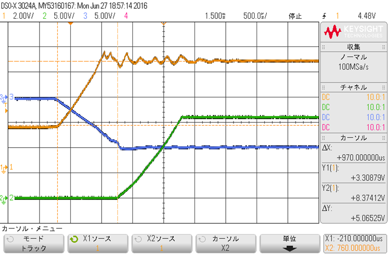
Is power up sequence timing depend on external charge pump circuit?

For example, below application note P2, use case of lower Negative Charge Pump.

※Boosting Positive Charge Pump is not use.

These sequence timing is attached, ch1 and ch3 ware the same timing.

※1ch:8.5V, 2ch:16V, 3ch:-10V

Best regards,

Satoshi

  • Hello Satoshi,

    Please send me the corresponding schematic and your requirements for the power up sequence (e.g: VO1 -> 1ms -> VO2 -> 1ms -> VO3)
    Thank you.
    Best Regards,
    Ilona
  • Ilona-san

    Thank you for reply.

    Basically, customer schematic is the same as attached circuit (page-3).

    2511979B_LCR6500_DMDBOARD_P65_1080P_S600_CSTACK_FLEX_CONN (5).pdf

    Difference point is one,  customer circuit is added  "Lowering the Negative Charge Pump" circuit.

    Best regards,

    Satoshi

  • Hello Satoshi-san,

    And what are the power-up requirements?

    Best Regards,
    Ilona
  • Ilona-san

    Sorry for my missing information.

    Power up requirement is based on DLP6500FYE.

    Please see attached below.

    ※VBIAS=8.5V, VOFFSET=16V, VREST=-10V

    Best regards,

    Satoshi

  • Hello Satoshi-san,

    The charge pumps are supplied by the SUP pin that is equal to the output of the main boost converter. This means that both charge pumps will start with some delay after the boost converter.  However the footnote 1) (below figure 17) in the d/s of the DLP6500FYE says that "..OEMs may find that the most reliable way to ensure this is to power VOFFSET prior to VBIAS during power-up ". 
    For the TPS65145 this means that AVDD (VOFFSET) needs to be powered before VGH (VBIAS) and this can be fulfilled with the current setup.

    For confirmation I will involve the DLP- Team to ensure that this start-up condition of the TPS65145 can work with the current design.

    Best Regards,

    Ilona

  • Satoshi-san,

    My name is Paul and I work with the DLP team. The schematics you included are from the Lightcrafter 6500 EVM. If the customer is using the TPS65145 as it is used in the EVM schematic, why do they want to add the lowering charge pump? VOFFSET, VBIAS, and VRESET all have fairly tight specifications as shown in table 6.4 of the datasheet.

    I agree with Ilona that the set-up should meet the power-up timing conditions for the DMD but I am concerned that the |Vbias-Voffset| will be too great if the charge pump is used. That difference can be no greater than 8.75 volts.

    Paul
  • Paul-san,Ilona-san

    Thank you for reply,
    And sorry for my late reply.

    The reason of lowering charge pump is -10V negative voltage.
    Application note "slva192", it was written in below on page 3.
    ⇒Lowering the Negative Charge Pump (|VOUT2| > VOUT1)

    Best regards,
    Satoshi
  • Satoshi-san,

    I don't understand why you're following the application note. The schematic you gave is a working and tested circuit that is perfect for the DLP chip that you're using. Why change it?

    Paul