This thread has been locked.

If you have a related question, please click the "Ask a related question" button in the top right corner. The newly created question will be automatically linked to this question.

TPS62560: TPS62560: TPS62560 going bad. SW node to GND resistance < 30ohms

Part Number: TPS62560

Hello,

I had created the same post (with same title) sometime earlier, not able to update as the post is locked, creating a new one.

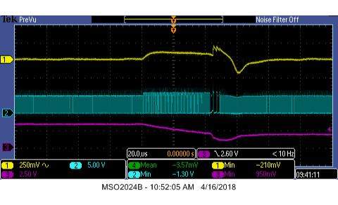
I am still facing the same issue. I have added some additional reverse voltage protection on the output of the regulator thinking reverse voltage is creating the issue, but I am still facing the same issue. Need some support on the same on priority.

Regards,

Avinash Aravindan

  • Hello Avinash,

    sorry for the late reply.
    I just had a look at your previous post, and it seems you were having problems with some electrical overstress killing the device during normal operation. The schematic and layout you shared are ok, but I also am concerned about two topics:
    -hotplug of the USB connector
    -fast and big variations of the digital resistor

    Did you already take care about those? In general, in order to shootout the problem causing the device's breakdown, you need to take some measurements of the voltages on the VIN and SW pin against ground with the oscilloscope. Can you show here some scope plots of the Vin and SW node during the application's operation?

    PS: in order to get meaningful measurements, please utilize the probing technique mentioned here:
    e2e.ti.com/.../2243.understanding-measuring-and-reducing-output-voltage-ripple
  • Hello Emmanuel,

    Thanks for the reply.I have captured the waveforms as suggested, attached the pdf with waveforms. I have captured all waveforms with active probes and short leads as feasible.

    Let me first explain the operating scenario and the failure scenario. The regulator is powered from USB supply and controlled by an MCU. The MCU will enable the regulator only when the user gives an input. The MCU controls the digital potentiometer in the regulator feedback path to set the output voltage to 5V, 3.3V, 2.5V or 1.8V as per user input. We have 5 failed units (out of 50), two of them failed at first power-up itself, 3 others failed when the voltage was varied (1.8V -> 2.5V - 3.3V - 5V) without any load connected. When the voltage is varied, the regulator voltage is first reduced to 1.8V in approx 60us (image 6 in the attached pdf) then ramped up to the required voltage.

    We have updated the schematics with an additional reverse protection circuit for the regulator, as we had observed the regulator getting damaged if a higher voltage is applied at the regulator output (which can happen in our usage scenario). Please find attached the updated schematics, the layout is exactly same for the regulator section.

    The first figure in the pdf shows VIN waveform while hot plugging USB, did not find any issues. The next 4 images are the SW waveforms for 1.8V, 2.5V, 3.3V & 5V outputs. Figure 6 shows the worst case ramp down of 5V to 1.8V in 60us. The remaining figures shows the different voltage transition waveforms (all captured at no load)

    Please let me know any additional details required. Please take this on priority, we are in a real tough situation with the product planned for production in Q3.

    Regards,

    Avinash AravindanTPS62560 Regulator Debugging.pdfTPS62560_schematics_2.pdf

  • Hello Emmanuel,

    Any updates?

    Regards,

    Avinash Aravindan

  • Hi Avinash,

    thanks for the detailed description, things get much more cleared that way. Indeed from figure 6 you can see that during the Vout discharge (with no load) the device is trying to discharge the Cout through the body diode of the HS switch (also called "boost mode" in this appnote www.ti.com/.../slyt689.pdf) charging the Vin cap and/or causing spikes on the sw node. By the way I asked also for the Vin waveform, which would have spotted the High Side switch body diode conduction and the spikes.

    The additional reverse current protection in not helping because if the current won't find a low impedance path to ground during "boost mode", but rather an high impedance (open path), then the voltage across the inductor (which is the source of that current) will increase the probability to have the breakdown.

    You can do one of the following two:
    -you work in PFM (R11 installed R14), which avoid this problem by simply letting Cout to self-discharge to the Vout target voltage
    -You need to act via software: control the slew rate of the Vout by programming small steps of resistance.
  • Hi Emmanuel,

    Thank you for your support, the problem seems to be exactly the same as you have mentioned. I have captured the waveform with VIN, The variation as mentioned is quite evident. I have attached the waveform which would be helpful for anyone referring to the post. We need to operate in forced PWM mode as we need tighter tolerance on the voltage at light loads, we will manage the same in software. 

    I have a few additional questions for my understanding as well as helpful for other referring to this post

    1) Why exactly the SW node is showing low impedance to GND after failure?

    2) Is there any calculation for the maximum allowable variation in voltage (V/us or something similar)?

    3) Is there any other hardware fix to avoid this issue (a diode from SW node to VIN for instance)?

    Regards,

    Avinash Aravindan

  • Hello Avinash,

    I'm glad you found out where the problem is. To answer your questions:

    1)During the faulty operation, because of the electrical overstress a breakdown event burns a junction between SW and GND, which will result in a short (almost).

    2)There is no similar recommendation. Anyway, based on your waveforms and schematic I can assume that the Cout average discharge current is:

    Delta(Vout)/Delta(t)*Cout=0.2A (almost, considering no load condition)

    I would try to limit this value by achieving the total Vout variation in a much larger amount of time. For example, one could limit to 0.02A with

    Delta(t)=Delta(Vout)/0.02A*Cout=500us (circa)

    You could use 0.1 V steps every 50us for a total Delta(V)=1V, for example.

    3) If you would use an external diode between SW and VIN you are just moving the current stress outside the device, but the overvoltage on the SW pin will still be present.
  • Hi Emmanuel,

    Thanks for the details, we have modified the firmware to vary the digital potentiometer one step at a time, which gives approximately 70us between each update. The worst case voltage variation is 50mV/70us. We did not observe any new failures (on 10 units). We are planning to build another 100 units and verify with the new firmware to be sure this has solved the issue and we are not missing any other corner cases.

    Regards,

    Avinash Aravindan

  • Hi Emmanuel,

    Even we modified the firmware and seems like solved the problem, but because we are planning to build another 100 units with TPS62560 recently so we want to 100% confirm what is the root cause. Therefore, could we send 1 pcs failed board to you for analyzing the root cause?

    Thanks.

    Regards,

    Tom
  • Hello Tom,

    I am sorry, but I can't accept this kind of support request, especially through E2E.
    You should contact one of our FAEs and discuss with them whether it makes sense to conduct a further investigation from our side.
  • Hi Emmanuel,

    Thanks for your reply. I bought these parts from Mouser and also asked them how to contact the TI FAEs, but they insisted we have to through the Techical support to get TI contacts. Could you tell me how to get the TI FAEs contact?

    Please let me know your comments.
    Thanks.

    Regards,

    Tom