This thread has been locked.

If you have a related question, please click the "Ask a related question" button in the top right corner. The newly created question will be automatically linked to this question.

BQ24610: BQ24610 Temperature

Part Number: BQ24610
Other Parts Discussed in Thread: BQ25713, BQ24773

Hello, This is Taehwan

I have a problem about BQ24610's Temperature.

I did check that this IC is very hot regardless of fast-charge values ex) 500mA, 1A, 2A

Condition is as below
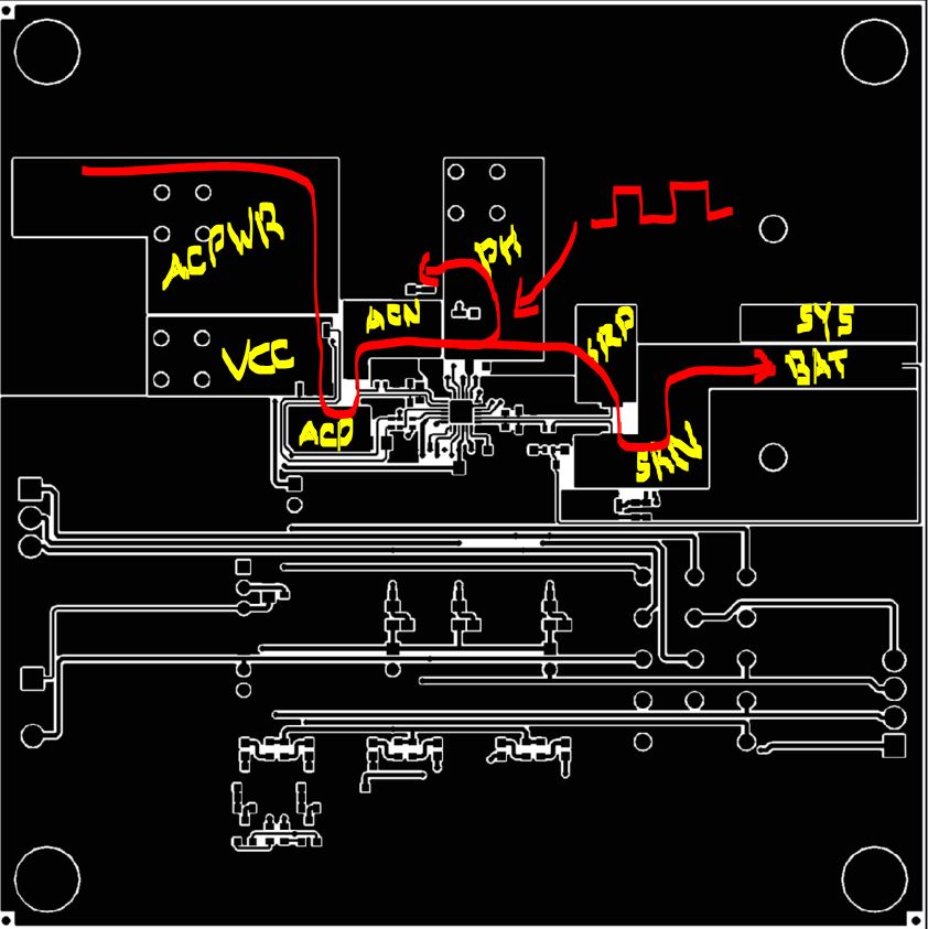
1) PCB is 2 layers

2) No seperate POWER GND with Signal GND

3) Vin=15V , Vout=13V

4) It is very hot but It work well.

Becuase of 1) and 2),Will this problem occur?

Why does it occur?

Additionally, Could you share datas about temperature according to fast charge current etc.

Please help me wih this problem.

Thank you for reading. 

  • Additionally, Is this IC very hot originally when it works ??
  • Hey Taehwan,

    It sounds like something is either improperly electrically connected or your component placement is too tight, resulting in excessively lossy components self-heating and heating devices around them, lack of thermal via'ing and all around poor heatsinking. 

    Take a look at this app note to help you optimize your board design: http://www.ti.com/lit/an/snva419c/snva419c.pdf

    Based on your testing configuration, the efficiency of the charger could be anywhere between 85% and 95%, considering your design didn't add a significant amount of extra power loss and matches our EVM fairly well. If so, @ 13.0V x 0.5A = 6.5W and those efficiencies, the power dissipated by the charger circuitry (BQ24610, sense resistors, input reverse current protection FETs, external power stage FETs, inductor, etc.) would be anywhere from 1.15W (low current) to 1.35W (high current). You can use the Theta_JA provided in each IC datasheet under a section called Thermal Information to get an estimate of the temperature increase in the IC, but do note that the power loss I calculated earlier will not typically be felt through the charger but moreso through the power components (HSFET, LSFET, and inductor). The IC is consuming mA's of current as compared to the other devices.

    Regards,

    Joel H

  • Hello Joel

    thank you for your detail information and data

    I think the efficiency of the charger is bad

    beacuse, Fastcharge is set to 2A, but measured Fast charge current is 1.6A.

    That is, efficiency of the charger is 80%

    this problem make hotter more and more.

    when This IC feeback 1.6A by current sensing, IC will work to make more and more current.

    so IC have high temperature.

    Is it right?

    so, I am finding to solve this problem.

    When it doesn't seperate  Power GND with Signal GND, Is Efficiency of ther chargher lower?

    or the other cause?

    For reference, I tried to extending  bottom's thermal GND, but it is very hot yet.

    please give me your know-how and skilled experience. 

    thank you! sir. 

  • Hey Taehwan,

    The efficiency of the charger is not so much that the power is heating up your board this much.

    Do you have layout you can share with appropriate schematic and symbol designators?

    I suspect you need either more thermal vias across the power planes, thicker copper, and even more likely many of your power components are heating each other and are very close to the IC.


    Regards,
    Joel H
  • Hello Jole

    Thank you your interesting.

    I attached circuit and layout.

    please help me

    Could you give me email?

    I can't attach files

  • I sent you a private message. Please send to that email.


    Regards,
    Joel H
  • hello joel.

    yesterday, i sent email to you

    please check the email.

    thank you

  • Yes I am reviewing the schematic and layout and will get back to you.


    Regards,
    Joel H
  • Hey Taehwan,

    I am looking at your layout based on your schematic. So I think with 1oz on a 2-layer board, you may be generating a lot of heat through overlapping traces. I imagine the heat dissipation is significant enough to process the 1 to 1.5W we talked about. However, I have some other concerns about noise-injection from the noisy power traces to signal traces routed underneath and under them like the gate drive signals. You also have the MAIN_RAIL for the SYS pin routed almost directly underneath the switching FETs as they trace back to the inductor.

    So I think we to look at the waveforms. If possible, please lift the inductor on one side and place a loop to measure the current through the inductor. We also want to look at the PH pin while the charger is switching and heating up. I would also like to see the LODRV and HIDRV voltages at the same time. We want to see if the FETs are switching fully on or if they are generating more heat than normal.

    And what is the DCR of your inductor and saturation current rating? Also, most inductor vendors provide a temperature vs. current data plot. We will likely need this information to determine if the inductor (which is very close to the IC; another point I wanted to highlight) is radiating heat to the charger and further increasing it's temperature.

    Another question is how much current is being pulled from MAIN_RAIL (VSYS) during your testing?


    Regards,
    Joel H
  • i sent you email

    please check email

    I appreciate your answer

    thank you Joel!!

    best regards

  • Hey Taehwan,

    Can you please provide a more zoomed in waveform of the PH, HIDRV, and LODRV pins?

    From the looks of the waveforms, it looks like the voltage is incredible low (Vpp) on the HIDRV, LODRV, and PH nodes. The PH nodes should be switching between the input voltage and ground. Your peak voltage is not even close to the 15V you are applying. This brings me to HIDRV and LODRV which whose voltage also look incredibly low.

    I suggest measuring the DC voltage you see on the REGN pin of the charger and tell me what you see.

    Also, once you provide the more zoomed in waveforms, we can see the voltages clearly on the PH, HIDRV, and LODRV.


    Regards,
    Joel H
  • thank you joel . i did try angain
    please chech the email
    thank you
    best regards
  • as you said, I did check about PH, HIDRV,LODRV, REGN again.
    PH is checked that high-level is 15V
    but I think they have some noise.

    because of noise, I think Fast charger current is lower than 2A. And , Is thermal efficiency bad?..Is it right?

    I sent you test result.
    the graph is normally? or not?

    How do you think about it..?

    Thank you joel!
  • Hey Taehwan,

    Can you zoom in further into those waveforms to show several at least a couple of switching cycles? Also, the waveforms look incredibly noisy so taking a closer look will help me see what is happening on those rising and falling edges of switching.

    DC-wise, REGN, HIDRV, and LODRV look fine but 32Vpp does not look good.

    From the layout, the thermal efficiency may be bad as the power stage is sitting right above the input rail. Basically, DC current is following both underneath the FET on the layer right below it and also through the FET. Another point is that FETs typically have a large thermal pad which again in your layout is sitting on top of the MAIN_RAIL (input) copper trace. Also, on a 2-layer, 1oz board the ability of these FETs to dissipate heat is very limited.


    Regards,
    Joel H
  • Hello joel

    I'm late. sorry

    we are designing the PCB.

    We plan to modify a number of layer that change 2 to 3 or 4 layer for avoiding Overlapping.

    and 1oz will be not changed.

    Nomally, What the number of oz do you recommend in battery charger PCB?

    Next,

    i can't understand your mention. because my English is bad.

    so please, help me with understaning

    1)From the layout, the thermal efficiency may be bad as the power stage is sitting right above the input rail

    Another point is that FETs typically have a large thermal pad which again in your layout is sitting on top of the MAIN_RAIL (input) copper trace

    -> It is not correct  that FET'S wide pad is sitting right above input trace. isn't it?, just thin Pins be connected with input trace?

    2)Basically, DC current is following both underneath the FET on the layer right below it and also through the FET

    -> DC current flow by FET and input trace. and BQ24610 is just sensing to flow constant current. and it converts Voltage level. right?...

      so, Current is lower than set 2A, because FET's efficieny has problem, right? or PG's noise?

    I already check  the temperature of the FET. but it is normal

    I tested that PG zoom in , as you mentioned.

    Please check the files.

    we can't attach files in Ti homepage. I don't know the cause.

    I will give you files on email.

    Could you recommend battery charger IC that Eiffieciency is over 90%?

    and normal state all battery charger IC is not hot . right?

    thank you for your detail mention

    Thank you Joel !.

    You are my savior!

    Thank you again and again.

  • Hey Taehwan,

    If you are only going to do a 2-layer board, at least 2oz to help with the heat dissipation for the power being processed.

    For 1) I took the two board images you sent and tried to overlap them. If you look at the two layers on top of each other you will find that specifically Q5 is on the top layer and directly over the MAIN_RAIL path that is on the bottom layer. Then the PH node also passes right above the MAIN_RAIL again on the top layer. The inductor is also very close to the IC as is the MAIN_RAIL.

    Separating the routing of the main power paths will help reduce heat generated. Also moving the charger away from these rails will improve the controller heat dissipation as well. As I've stated before, this is a charge controller and it does not directly process any power so it should not be at all hot. This points to the layout causing the extra heat generated around the device.

    Another thing to check for is the potential shorts to GND or low impedance paths from the input to GND or BAT. You may want to test an unpopulated PCB and check the resistance between those nodes.

    I have also attached the example EVM layout here for your reference. First note that we used a 4 layer board for this design. Secondly, note that the main power paths are not overlapping each other on other layers and that the BQ24610 controller is somewhat isolated from these paths.

    For 2) While the FET temperature is normal, it is possible it is dissipating all of its heat into the FR4 dielectric material between copper layers, and because the copper is so thin at 1oz it is making its way to the MAIN_RAIL. Additionally, I would imagine the inductor heat dissipation is playing a role here.

    The best thing for you to check would be a thermal/IR camera to look directly at which components and what areas of the board are getting the hottest.

    For slightly better efficiency, look at the BQ24773 and the BQ25713 charge controllers. However, even with these you can likely experience the same problem if the layout has the same issues.

    Regards,

    Joel H

  • Hello Joel.

    This is Taehwan

    Very very Thank you so much your detailed explanation.

    It was very helpful.

    I am improving to PCB refering to your mentions

    I will test new board next month. so I expect that PCB is good.

    Thank you so much , Joel.

    Happy new year  and Merry christmas