A related question is a question created from another question. When the related question is created, it will be automatically linked to the original question.
If you have a related question, please click the "Ask a related question" button in the top right corner. The newly created question will be automatically linked to this question.
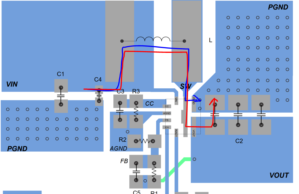
1. Please refer to the recommended layout in the datasheet. The most critical current path for all boost converters is from the swithching FET, through the synchronous FET, the output capacitors, and back to the ground of the switching FET, The output capacitors and their traces should be placed on the same board layer as the IC and as close as possible between the VOUT and PGND pins of the IC.
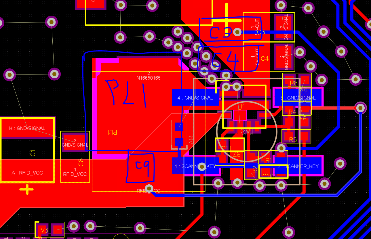
2. There is a polyregion on PL1, It should be removed. Place C9 close to U1 and supply a stable Vin voltage. Place C3,C4 close to VOUT, GND pins of the IC.