This thread has been locked.

If you have a related question, please click the "Ask a related question" button in the top right corner. The newly created question will be automatically linked to this question.

UCC27201: IHB current measured as 300uA total between two FET Drivers. A higher IHB could cause our circuit to fail. Want to make sure it won't.

Part Number: UCC27201

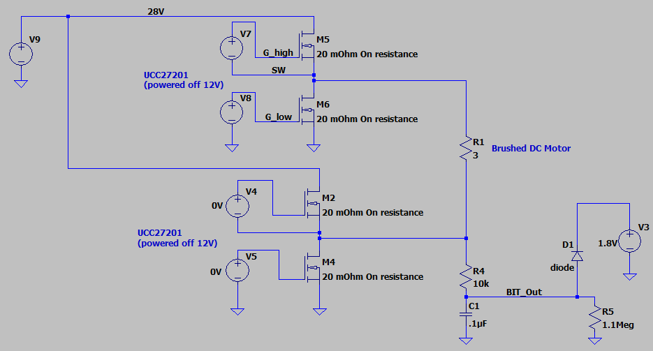
We use two UCC27201 to drive two half bridge in an H-bridge configuration for a brushed motor control. The voltage on the H-bridge could be between 18V and 28V. We have an RC circuit (10kohm and .1uF) connected to one one side of the brushed motor to test if the FETs are good (a built in test). We turn on one FET at a time and look at the output of the RC. For each Half-Bridge we turn on the low side FET for 2mS to charge the boot strap capacitor, and cause the output of the RC to be 0V. We then test the high side FET by turning it on, waiting 400uS and then measuring the voltage. If the voltage rose to above 1.75V the HS FET passed (clipped by a diode to 1.8V). We then turn on the LS FET for 2mS, read the voltage and verify it's below 1.25V to make sure the LS FET is good. The issue I'm concerned with is a false pass on the HS FET due to IHB charging the capacitor and making it look like the HS FET came on when it did not. The concern is if IHB is large enough it will cause the capacitor to charge from 0V to 1.75V within the 400uS. My spice simulation shows that if the total IHB (between the two FET drivers on the H-bridge) is more then 550uA then under worst case temperature (125°C, 75nF capacitance = .1uf nominal with -15% X7R, -10% aging).

Note: When I run a bench test the circuit works (IHB is not charging the capacitor fast enough during the 400uS given the HS FET did not come on like it was supposed to) and I'm only measuring 300uA going through the 10kohm resistor when all FETS off. 

My question is do I need to worry about the worst case spec of .8mA IHB per FET = 1.6mA total between two FET drivers (again, my sim shows anything over 550uA with 75nF capacitor will cause the voltage to rise enough within the 400uS to cause a false pass on the HS FET). Again, I only measured 300uA total between the two FET drivers which does not coincide with the .4mA x 2 = .8mA typical value in the datasheeet.

Thanks,

Nick

  • Hello Nick,
    Thank you for the interest in the UCC27201 half bridge driver in your application. After reviewing the datasheet I see that the typical IHB is specified as 400uA which is less that you reference in your bench test.
    The datasheet can be found here: www.ti.com/.../ucc27201.pdf
    If you review the typical characteristic curve Figure 21 you can see that the IHB and IVDD vary with VDD and VHB supply voltage. It sounds like in your test case, the VHB is likely at a lower voltage than the parameter table condition of 12V.
    What is the VDD voltage in your application? This will have an impact on the quiescent currents.
    For the condition of VDD and VHB=12V the quiescent current of 0.4mA typical and 0.8mA maximum were specified during product development based on test data and simulation data to accommodate temperature and process variation.
    Based on this, we cannot guarantee that the IHB quiescent current will be less than the specified value in the datasheet over temperature and all devices.
    Something that is not clear. It seems with 2ms on time of the low side that the HB capacitor should be fully charged. If the VDD level is 12V it seems you should see closer to 400uA IHB when the HB capacitor starts discharging.

    Regards,
  • Thanks Richard,

    Sorry for the late reply. 

    VDD = 12V and voltage on Bridge = 28V. To clarify: the motor (about 1.5 ohms) is connected between the two half-bridges (to make an H-bridge). The RC is on one side of the motor only. So the current through the R should be the IHB combination of both UCC27201 chips (one for each half bridge as the IHB for one of the UCC27201 should go through the motor to the RC). Thus I would think I would be measuring 400uA x 2 = 800uA through R. However, as mentioned, I'm only measuring 300uA through R.

    Something I'm trying to understand. In my case I have an RC that can sink the IHB to ground until the C charges. However, if nothing is connected between the half-bridge switch node (UCC27201 pin 4) and ground what path does IHB take to ground?

    On that note: because I have an RC (and not a direct short to ground) does this affect it i.e. is part of that IHB taking another path to ground?

    thanks,

    Nick

  • Hi Nick,

    Sorry for the delay. Richard will get back with you on Friday.
  • Hello Nick,

    To make sure I understand the possible path of the IHB current, can you provide a schematic of the driver, motor winding connections and the sensing RC circuits?

    For the HB capacitor to charge there needs to be a path from VDD thru the boot diode into the HB capacitor. For the HB capacitor to fully charge and  the HB-HS voltage to reach the maximum value, there does need to be a path from HS to ground resulting in the HS pin being near ground.

    If the motor winding is connected to the HS terminal and the other winding termination to ground the winding resistance would be the path to ground.

    I assume however, that one winding terminal is connected to the HS pin of one driver, and the other winding terminal is connected to the other driver HS pin.

    In this case the motor winding resistance would not be a resistance to ground.

    It is still not clear, what the HB-HS voltage level is during this test sequence is. As I mentioned before, The IHB current is less with lower VHB-VHS than is in the parameter table 12V test condition.

    Can you provide a schematic showing the details? It can be a simplified schematic if you prefer. Also can you measure the differential VHB-VHS voltage during the condition where you measure less than 550uA total current?

    Regards,

    Richard Herring

  • Hi Nick,

    It's been a while since we've heard from you, so we must assume you've resolved your issue.

    If possible, please post how it was resolved for others to learn from.

    If your issue isn't resolved, let us know, and we will work with you to resolve it.
  • Hi Richard,

    Sorry for the late responses. i'm trying to squeeze this in with another couple projects but want to continue to a resolution. I've inserted a simplied circuit as I can't show the design. i will try to get in the lab and 

    measure the VHB-VHS you mention this week. I did measure the VGS of the high side FET and I believe it was around 11.5V. The current I was measuring was through R4 in the picture.

    Thanks, Nick

  • Hello Nicholas,
    I will make some assumptions on the driver connections to the circuit shown and will describe the assumption.
    The driver on the top side have the HS pin connected to the M5 source/M6 drain, confirm if that is correct.
    For the HB capacitor to charge, either the M6 needs to turn on forcing SW note to ground which is what I recall is the test sequence. If LO is not turned on, the charging path will be 12V UCC27201 VDD thru the internal boot diode to the sum of R1 and R4, to the parallel of C1 and R5.
    The HO is turned on for 400us as part of the test based on earlier description. Can you provide the capacitor value on HB-HS, as this seems like a long time to sustain the HB-HS bias.
    Waveforms of the HB, HS, HO and LO will be helpful to confirm the high side bias operation.

    Regards,
    Richard Herring
  • Yes, the UCC27201 HS (pin 4) is connected to M5 source/M6 drain. Yes, the low side FET gets turned on (LO = pin 9 on UCC27201) to charge the HB capacitor (2 mS) as noted in the test sequence. The capacitor between HB (pin 2) and HS (pin 4) is .47uF. I will try to get you waveforms later this week.

    thanks,

    Nick