This thread has been locked.

If you have a related question, please click the "Ask a related question" button in the top right corner. The newly created question will be automatically linked to this question.

TPS2113A: Output Voltage unstable when input changed

Part Number: TPS2113A
Other Parts Discussed in Thread: TPS2112A

Hi E2E,

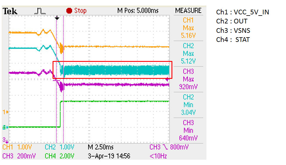
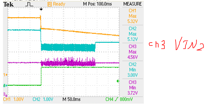
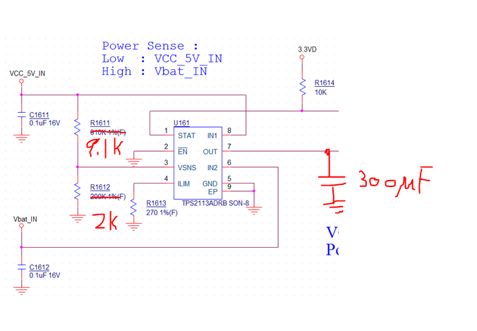
Power Mux circuir as below

(1). VCC_5V_IN : Main power (Adaptor 5V) 

(2). Vbat_IN : Battery (3.6~4.2V) 

Avg. System power consumption : 5V / 820mA

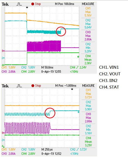
IN2   : use power supplier 4V/1.6A to simulate
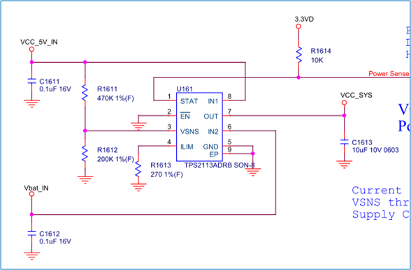
Question: 

Why OUT pin (Ch2) will unstable 225ms when STAT changed ?

  • Hi Julian, 

    Thanks for reaching out on E2E!

    Can you also capture IN2 during the switchover event? It looks like the device is trying to toggle between IN1 and IN2 during the initial switchover event. You could also try to reduce the resistor divider such that the switchover happens when IN1 dips lower.

    As described in Output Voltage Slew-rate Control section on page 17:

    High inrush currents can glitch the voltage bus and cause a system to hang up or reset. It can also cause reliability issues—like pit the connector power contacts, when hot-plugging a load such as a PCI card. The TPS2112A/3A slews the output voltage at a much faster rate when OUT switches between IN1 and IN2. The fast rate minimizes the output voltage droop and reduces the output voltage hold-up capacitance requirement.

    Also, what is the output capacitance and output current load for the application? Perhaps the thermal shutdown is being engaged due to a large amount of power being dissipated during the switchover. 

    Thanks,

    Arthur Huang


    To find the latest information on Power Switches, visit www.ti.com/powerswitch

  • Hi Arthur,

    Thanks for you reply!

    OUTPUT = 5V/0.8A

    Cout is 10uF

    I think that is "High inrush currents can glitch the voltage bus and cause a system to hang up or reset."

    So How do I improve it? add more COUT or reduce the resistor divider or BOTH?

    Thanks!

  • Hi Julian,

    Yes, I recommend both reducing the resistor divider and increasing COUT. It looks like CH3 is toggling during the initial switchover event, which could be caused due to the sudden change in current (I = C * dV/dT). Adding more input capacitance to IN2 should also help in this scenario alongside the R divider and COUT.

    Thanks,
    Arthur
  • Hi Arthur,

    Thanks to your reply.

    We modify the circuit as below,

    After we test it, the waveform no any improve yet.

    I have 2 question about this case:

    1. I think that when IN1 change to IN2 what can't avoid the inrush current. So do we have any method to keep VOUT stably?

    2. The red circle of the waveform. Does IC limit current lead to VOUT  be clamped?

    3. If we ILIMT set 0R to GND that just for keep VOUT stably. Does it have any risk?

  • Hi Julian,

    Sorry, I mean to reduce the resistor ratio even further to allow for IN1 to dip further before switching over. My thoughts are that during the switchover event from IN1 --> IN2, IN1 will start ringing since the current is suddenly changing and you could be using longer cables (V = L * di/dT)

    Can you try adjusting the resistor ratio even further on the VSNS pin?

    You can also keep IN1 and IN2 more stable by adding additional input capacitance to reducing the ringing during the switchover event.

    If you set the RILIM resistor to GND or 0Ω, then the current limit feature will be disabled. I don't recommend this feature unless your downstream load can withstand no current limit.

    Thanks,
    Arthur