This thread has been locked.

If you have a related question, please click the "Ask a related question" button in the top right corner. The newly created question will be automatically linked to this question.

TPS56637: Stability vs. Recommended Values for Output Filter and Feed Forward Components

Part Number: TPS56637

Hi TI Team,

We are designing a 5V-to-0.8V and 5V-to-1.8V converters using the TPS56637. This is our first attempt at designing with the D-CAP3 architecture. Our design requires a very low PDN impedance across a large frequency range. As a result, we have a fair amount of decoupling on the output. Table 4 of the datasheet (p. 19) has recommended values for a maximum Cout of 100uF. Our output capacitance exceeds that by several hundred microfarads. Additionally, the range given for the feed-forward components (C9 and R8) is somewhat restrictive.

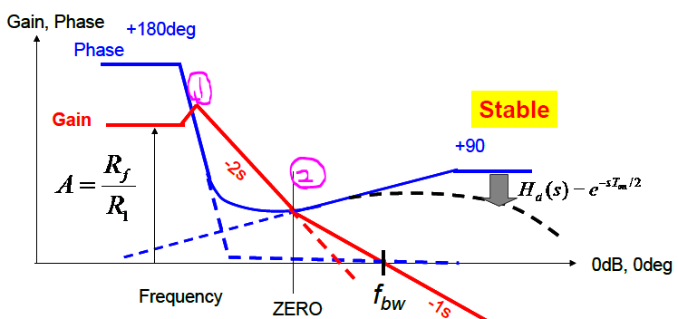
The datasheet does not go into any detail about the stability details and the ramifications of component values going outside of the recommended range. Could you please provide details about the control loop stability and how to deal with much larger output capacitance without impacting the design stability?

Thanks very much,

B. Assar

  • Hi Assar,

    All the decoupling cap are put in local? Can you upload your SCH for review?

    For the stability control, we can see below typical DCAP2/3 frequency response. At marked 1 point, there is the LC double pole, Fpole=1/[2*pi*sqrt(LC)]. At marked 2 point, there is internal ripple injection zero, which is fixed internally in DCAP2/3. So if C or LC is large, the LC double pole will be small and make the Gain cross the 0dB with -2s slew rate (-40db/dec) as shown by the red dash line. In such situation, the system will be unstable.

    There is a way we can have a try. Using large output cap and small inductor, it will improve the stability but inductor current ripple or output ripple may increase, what's more we also need to consider peak current with small inductor whether it will trigger OCL. So we need to know your application request, input and output voltage, max output current, output ripple requirement...

    For the feedforward components, datasheet linked an application note "Optimizing Transient Response of Internally Compensated DCDC Converters with Feed-forward Capacitor" on the bottom of Table 4 which is helpful when designing feedforward. 

      Thanks,

    Lishuang

  • Hi Lishuang,

    Thanks very much for your quick response. It's much appreciated.

    We are actually planning to use the TPS56637 for six different rails (schematics attached for your review). If I understand your explanation correctly, we need to maintain the corner frequency (Fpole) around 10kHz, which means for larger output capacitance, we have to select smaller inductance (which as you pointed out leads to larger rippler current). I suspect this may not be practical for a couple of our rails because of the large amount of capacitance on the output. I will wait for your feedback.

    Please note that the bulk capacitance placed at the output of the regulator is on the same page as the regulator. The bulk and bypass capacitance placed at the ASICs are shown in the final pages of the schematics.

    A follow-up question is the determination of Fbw. Based on PSPICE simulation results of transient response, I see in some cases, the bandwidth seems to be close to 100 kHz! That seems very large. Is it possible that I am misinterpreting the result? Below is an example (Vout=0.85V, load step 0 to 3A).

    TPS56637_for_TI_Review.pdfThanks and regards,

    B. Assar

  • Hi Assar,

    Your understanding of LC Fpole is correct. For larger output capacitor, we need to use smaller inductor so as to make LC double position don't change a lot according to LC recommendation table. Smaller inductor can make inductor current ripple large, but output ripple will be small as a results of large amount of capacitors. 

    According to your SCH and your description above, 47uF*8 capacitor are put in local, others at ASICs side, am I understanding right?

    Out TPS56637 band width can be up to 100KHz-200KHz.

    Thanks,

    Lishuang

  • Hi Lishuang,

    Thanks again for the quick response. You are correct about the output capacitance. Each design instance has eight 47uF caps placed right at the output of the converter.

    If we do not reduce the inductor value, will we see any stability problems?

    Also, we notice that with changing the load current, the cross-over frequency shifts along the frequency axis (typically between 7 and 12 kHz). What is the explanation for this? It doesn't take a dramatic change in load current (say, 0.5A) for the cross-over frequency to move!

    Thanks and regards,

    B. Assar

  • Hi Assar,

    If so, the system can be stable with current setting without changing the inductor value.

    I don't have much experienced in PSPICE simulation variation analysis. But when we do bench test using frequency analyzer, even with same condition and same board, the bandwidth and phase margin of two time test will also have a little bit difference. If only have 7-12KHz shifts of bandwidth, it is okay.

    I also checked your SCH, two recommendations:

    1. Add one 0.1uF input cap to filter high frequency noise. Or change 1uF to 0.1uF.

    2. The feedforward cap, for example C5001, can set to 100pF first.

    Thanks,

    Lishuang

  • Hi Lishuang

    Thanks for your effort in reviewing the design and your feedback.

    Regards,

    B. Assar