Other Parts Discussed in Thread: LM25149-Q1, LM5146-Q1, LM5143-Q1, LM5164
Hi there,
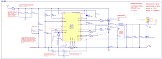
I have an LM5116 design that operates on 48-85Vin, 12Vout, 1.5A.
I'm trying to reduce the amplitude of the ringing on the switch node, as the peak exceeds 100V when operating at Vin = 85V.
I have based my layout on snva803 by:
- Placing input capacitors as close to the MOSFETs as possible.
- Using 3mmx3mm package MOSFETs for low parasitics with a low Qrr value.
- Keeping the main power loop area as small as possible.
- Generally making the layout as tight as possible.
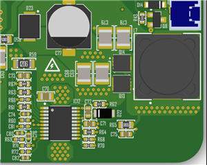
With the circuit schematic and layout attached, the switch node ringing exceeds 100V - measured using a ground clip, not the long ground lead.
I have made the following changes to the schematic to try and reduce the peak of the ringing:
1) Increased the HS gate resistance from 0Ohm to 20Ohm - reduced peak from 109.3V to 101.3V.
2) Added an RC snubber circuit to the switch node, 2.2Ohm and 100pF - reduced peak to 98V.
Here is what the SW node looks like (the snubber did a good job at dampening the ringing):
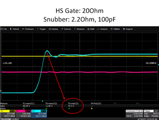
I would like to reduce the ringing further. Considering the input voltage is 85V, ideally I would like to get the ringing down to <95V, as I've found the LM5116 is the first components to fail if the input voltage rises slightly above 85V.
I don't think there are significant flaws in my PCB layout, would you agree?
Is there anything else I can try to reduce the peak of the ringing, if it's a MOSFET issue, what MOSFET parameters should I pay the most attention to?
Any help would be greatly appreciated!
Ben