A related question is a question created from another question. When the related question is created, it will be automatically linked to the original question.
If you have a related question, please click the "Ask a related question" button in the top right corner. The newly created question will be automatically linked to this question.
Can you check the OSC output to verify that the oscillator is running normally?
I would also check the PID OUT signal and the output of amplifier
Are you trying to use the on-board error amplifier as a unity gain buffer and have the control input come from the external error amplifier U6B ? If so then pin 1 and pin 9 of the UC3525 should be connected as you have shown but the control input from U6B should go to pin 2 of the amplifier. The connection from Vref to pin 2 is not needed.
I would try to run the system open loop - as Ben suggested.
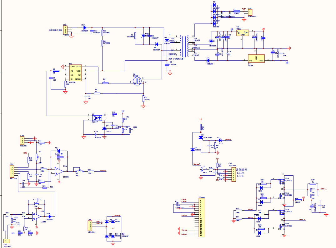
Dear Ben; Have Add main board schematic diagram. Please See Above. And also tested KA325. It just happens occasionally when using KA3525. So suspect it was caused by external disturbances.
Thanks for the additional information. Were you able to test the circuit in open loop? Do you see abnormal behavior at the oscillator output? Do you see any noise on the IN- pin?