


Part Number: 66AK2H06
Hello!
We are in process of bringing up custom board with 66AK2H06. Though we looked at EVMK2H for reference, our design does not copy evaluation board one to one.
Consider clock domains as per http://wfcache.advantech.com/www/support/TI-EVM/download/XTCIEVMK2X_Technical_Reference_Manual_Rev1_0.pdf, Figure 2.2:
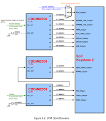
This picture specifies ARM_CLKp/n to be 125MHz and SYS_CLKp/n as 122.88MHz.
We refer board management controller (BMC) from Advantech site http://wfcache.advantech.com/www/support/TI-EVM/Rev4_0/BMC/BMC_EVMK2K_1_0_2_6-20160330.zip. One thing I'd like to clarify is BOOTMODE pins values. In ks2evm-bmc-v1.0.2.6\bmc\src\bmc_state.c there is a definition:
static BOOTMODE BOOT_MODES[16] =
{                                                                // DIP
    {0x00000000, 0x00110CE7, "ARM NAND"},                        // 0000
    {0x00000000, 0x00100001, "DSP No-Boot"},                     // 0001
    {0x00000000, 0x00112005, "ARM SPI"},                         // 0010
    {0x00000000, 0x00100003, "ARM I2C"},                         // 0011
    {0x00000000, 0x00100CEF, "ARM UART"},                        // 0100
...
Consider "ARM_NAND" mode, which is defined as 0x00110CE7. These values define BOOTMODE[15:0] pins and LENDIAN input. As far as I have traced from the code, LSB of the config word, which is 1 for all configuration, is LENDIAN value, and one makes the system little endian. Then upper bits would match bootmode values as per table in Figure 10-1. DEVSTAT Boot Mode Pins ROM Mapping in K2H datasheet.
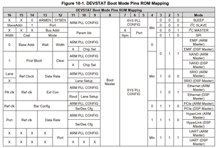
So I make following mappings for 0x00110CE7:
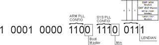
Here I decode SYS PLL CONFIG as 0b111 and ARM PLL CONFIG as 0b110. Then according to Table 10-27. System PLL Configuration and Table 10-28. ARM PLL Configuration
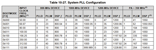
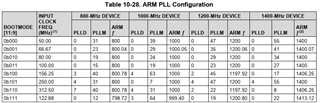
I am happy enough with SYS PLL CONFIG as 0b111 makes top clock speed for DSP out of 122.88MHz clock, just as explained in Advantech manual. However if we look at ARM PLL CONFIG, its value of 0b110 tells that top speed of ARM core would be produced out of 312.50MHz clock. However, clocking diagram in Advantech manual (that one with blue CDCMs) shows ARM_CLKp/n is 125MHz. This value would produce less than half of top ARM clock speed.
I could be missing something terribly important, so asking experts to clarify and guide me through this.
Thanks in advance.