This thread has been locked.

If you have a related question, please click the "Ask a related question" button in the top right corner. The newly created question will be automatically linked to this question.

AM4378: MIN values for Input signal rise time and Input signal fall time

Part Number: AM4378

Hi Support Team,

I have questions about the MIN values for Input signal rise time and Input signal fall time.

Q1: Regarding Input signal rise time and Input signal fall time in the datasheet "5.12.17.1 MMC Electrical Data and Timing",
is it necessary to strictly observe the MIN value of 1ns?

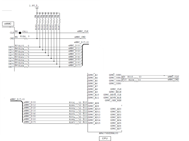
The current schematic is as follows.

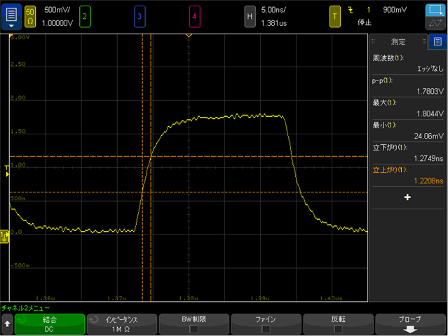
The waveform of DAT3 from eMMC to CPU is shown below.

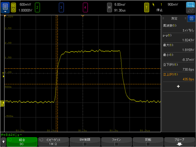
The time axis scale has not been expanded in relation to the transition time, but it is within 400 to 500 ps.
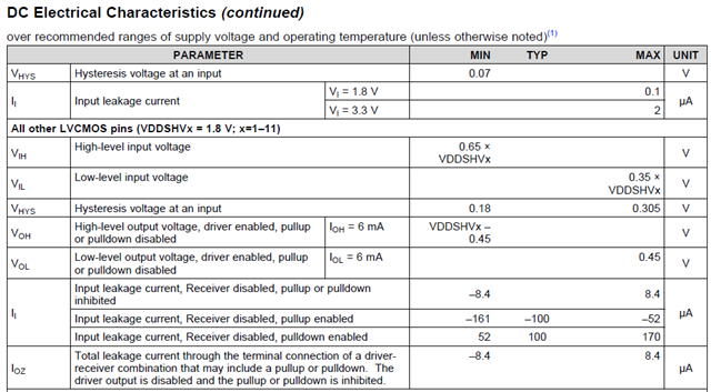
The thresholds for rise time are as follows
VILmax: 0.65*1.8=0.63V
VIHmin: 0.35*1.8=1.17V
*Used with 1.8V VCCQ


The waveform after the constant change is shown below.


The constants after the change are as follows

Damping resistor on CPU side: 56Ω
Damping resistance on eMMC side: 100Ω
External pull-up resistors on CMD and DATA (7:0) lines (pull-up near eMMC): 10 kΩ


Q2. I checked the following thread. is the rise time specified from 10% to 90% instead of VILmax to VIHmin?

e2e.ti.com/.../am437x-input-signal-rise-time-and-fall-time-from-nand-flash-memory

For eMMC, JEDEC stated VILmax to VIHmin, so we measured the same period.

Best regards,
Kanae

  • Q1: Regarding Input signal rise time and Input signal fall time in the datasheet "5.12.17.1 MMC Electrical Data and Timing",
    is it necessary to strictly observe the MIN value of 1ns?

    A1. The input rise/fall times defined in the Timing Conditions table were used as the input signal limits when the MMC peripheral was timing closed to meet all Timing Requirements and Switching Characteristics defined within this section of the datasheet.  Your customer is expected to perform a timing analysis of their system implementation, where they consider the timing requirements of each device when taking into consideration the combination of PCB delays and switching characteristics of the sourcing device. They should not have a problem with a faster rise/fall time if their system has more than enough margin to account for the difference between the actual min rise/fall time and the min rise/fall time listed in the Timing Conditions table.

    Where was the customer probing the DAT3 signal when measuring the rise time shown in the attached waveforms?  I ask because the rise/fall time is different based on where you place the probe along the transmission line. They need to be probing at the AM437x pin. I would also like to know how they were sure these waveforms properly represent the signal rise time when being driven by the eMMC device rather than driven by AM437x.

    Q2. I checked the following thread. is the rise time specified from 10% to 90% instead of VILmax to VIHmin?

    A2. I think the other thread is correct. Our timing closure team most likely used 10% to 90% instead of VILmax to VIHmin.

  • Hi Paul,

    Thank you very much for your reply.
    Regarding your questions, I will check with the customer,
    so it will take some time for us to get back to you.

    Best regards,
    Kanae

  • Hi Paul,

    Customer measurement points are as follows.


    He has a damping resistor at the following location on the wiring pulled out from the AM437x terminal,
    and we are measuring at the pad of the damping resistor.
    The distance from the terminal of AM437x to the pad of the damping resistor is about 6mm.

    The customer's verification that these waveforms are the rise time of the signal when driven
    by an eMMC device is based on the following.

    After running a test program to read data from an eMMC, it was confirmed
    that the signal is driven by an eMMC device based on the phase relationship with the CLK.
    In the case of driving by the CPU, the DAT change is confirmed at the same time as the falling edge of the CLK.


    <Paul>
    A2. I think the other thread is correct. Our timing closure team most likely used 10% to 90% instead of VILmax to VIHmin.


    My customer is on the understanding about your answer; A2.
    His additional question is here.

    Q. Just to confirm, am I correct in understanding that the rise and fall time of the input signal of each peripheral
    of AM437x is specified in the range of 10% to 90% regardless of MMC?

    I checked the rise and fall times again under the following conditions for the 10% to 90% period,
    and the results were 1.9ns rise time and 2.6ns fall time, which is within the 1 to 5ns range described in the datasheet.

    [Constants prepared at the time of board design]
    -Damping resistance on eMMC side: 0Ω
    -Damping resistance on CPU side: 33Ω


    I am waiting for your reply to an additional question.

    Best regards,
    Kanae

  • The rise/fall shape is typically distorted at the near-end, where it will have a discontinuity at approximately mid-supply. I was almost certain the signal being measured was being probed near the far-end of the transmission line based on the rise/fall shape. However, I wasn't sure where they were probing the signal. Looking at the data transition delay relative to clock is another good way to confirm the transition capture was the result of the eMMC sourcing. Based on the above information, we are now certain the rise/fall being measure is the AM335x data input signal.

    AM335x is a very old design, so it may be difficult to get a firm answer. My previous comment was based on the approach we use today. I suspect the process has not changed since all of our IO timing models are based on 10/90 voltage limits. When performing timing closure of a peripheral, we convert any rise/fall time requirements of industry standards/specifications to a slew rate using the specified voltage limits then apply the slew rate to our 10/90 limits. This effectively scales the rise/fall times requirements from industry standards to match our model.

    I'm glad to see your customer is being very diligent in confirming there system is compliant to our timing requirements, but it is rare to encounter any timing risk when violating the minimum rise time since this time is typically small and any violation is even smaller. Many of the peripherals do not require us to define a minimum rise/fall time for timing closure, but the timing closure tool being used requires a minimum and maximum value. In those cases, we typically use a value that is smaller than we feel is possible in a real system.

    Regards,
    Paul


  • Hi Paul,

    Your reply does mention AM335x, but my customer is using AM4378.
    Is AM335x wrong for AM437x?
    Am I correct in understanding that your answer is also about AM437x?

    Best regards,
    Kanae

  • I'm sorry for the confusion, my reply is still valid since AM335x and AM437x are built using the same technology node and use the same IO designs.

    Regards,
    Paul

  • Hi Paul,

    Thank you for your prompt reply.
    I will now share it with my customers as an answer to AM437x.

    Best regards,
    Kanae