


Part Number: AM4378
Other Parts Discussed in Thread: TLV320AIC3104,
Hi Support Team,
My customer has the following question regarding McASP for AM437x processors.
We are checking the operation on a prototype board, and we believe that there is a problem
with the way McASP works and the connections that were assumed when the board was created.
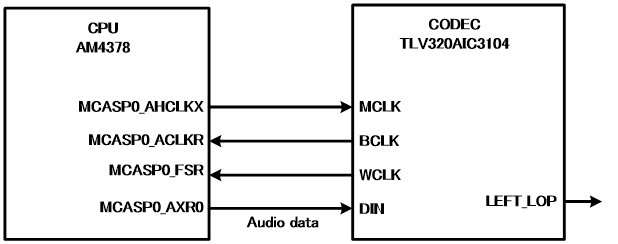
The connection relationship between the CPU (AM4378) and CODEC (TLV320AIC3104) that
was originally planned is as follows.
-Supply MCLK from CPU to COEDC
-CODEC operates in master mode
-Supplies BCLK and WCLK divided in CODEC to CPU
-Output audio data from CPU to CODEC
-DA audio in CODEC is played back through speakers via AFAMP
Reference diagram: originally planned connection
My understanding was insufficient at the time of design, but I have rechecked
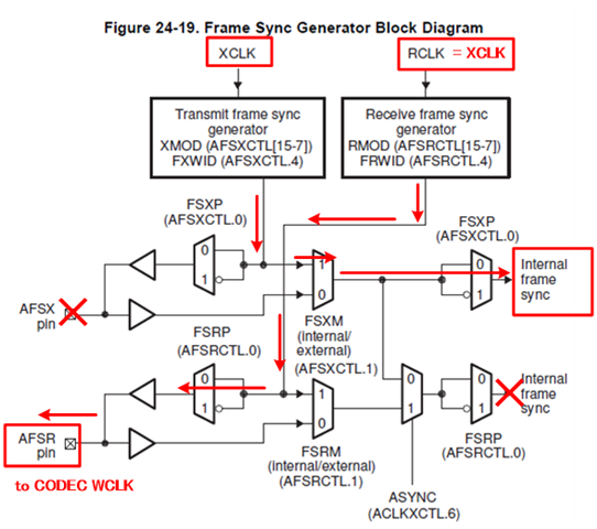
the AM437x Technical Reference Manual "24.3.5 Clock and Frame Sync Generators"
and the Application Report SPRACK0, and have the following confirmation/questions.
Please answer the following questions.
Q1. Are each of the following recognitions correct?
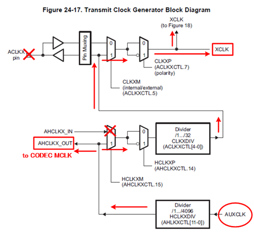
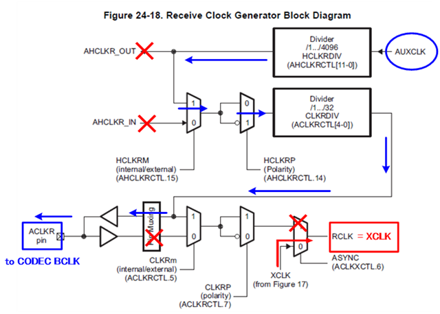
-To output data from the CPU to the CODEC, routing to the internal data transmission XCLK and internal frame sync is required.
-CLK input from outside to the MCASP0_ACLKR and MCASP0_FSR pins can be routed to RCLK and internal frame sync for reception.
The XCLK and Internal frame sync cannot be routed to the XCLK and Internal frame sync for transmission, and thus cannot be used in the expected manner.
-For example, if BCLK and WCLK from CODEC were connected to MCASP0_ACLKX and MCASP0_FSX pins,
they could be used in the configuration originally envisioned.
-Since MCASP0_ACLKX and MCASP0_FSX are capable of routing not only to transmit but also to receive RCLK
and internal frame sync, BCLK and WCLK can be routed to MCASP0_ACLKX and MCASP0_FSX regardless of the data transmission
or reception, master mode or slave mode configuration. ACLKX and MCASP0_FSX could be used as long as they were connected.
Q2. If we want to support this without modifying the board, is it possible to use the following configuration?
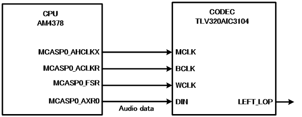
The signal input/output relationship should be as follows: CPU as master, CODEC as slave mode,
and the routing of the McASP clock inside the CPU should be as follows.
In the block diagram of Transmit and Receive, it is assumed that the frequency divider ratio of Divider is aligned.
AUXCLK is shown in red for transmit and blue for receive in the figure below,
but it is assumed to be synchronized if the source is the same.
Transmit Clock Generator Block Diagram
Receive Clock Generator Block Diagram
Frame Sync Generator Block Diagram
Please excuse this configuration, which is not usually used.
However, we need to consider whether it is possible to handle this without modification of the board.
Immediate support for the above question would be greatly appreciated.
I would like to have your prompt reply, or a schedule of this reply at least.
Best regards,
Kanae
