Other Parts Discussed in Thread: SN74AUC1G19
Hello,
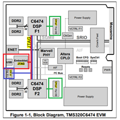
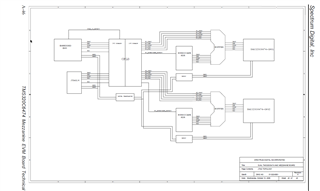
Our company is still using "TMS320C6474 Mezzanine EVM Board" and recently Spectrum Digital stopped manufacturing these boards.
We managed to acquire the PCB layout, schematics and BOM for this specific card as an option in case we want to manufacture them.
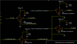
The drill that those resources are missing the embedded emulator circuit, the BOM and schematics dont include any thing related to the embedded emulator circuit.
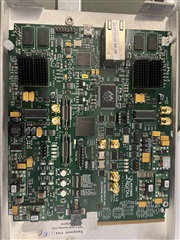
Card with embedded emulator
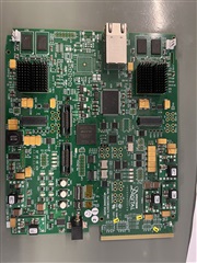
Card without the embedded emulator
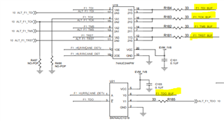
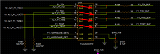
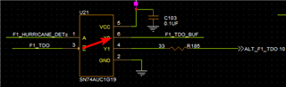
Now according to JTAG TOPOLOGY there some kind of detection of which kind of JTag connection is being used.
My question is: is it possible to connect via JTag 60PIN to DSP using XDS 560 v2 Emulator without the existence of the embedded emulator Circuit?
if no, can you specify the reason?
if yes, how? (hints are welcome)
Thanks,
Boutros Farah