This thread has been locked.

If you have a related question, please click the "Ask a related question" button in the top right corner. The newly created question will be automatically linked to this question.

TMS320C6657: My own made board power up problem

Part Number: TMS320C6657

I made my own board using TMS320C6657.
My developing envirement is CCS5.5 IDE with XDS2xx USB Emulator.
My board's power sequencing is IO-before-Core just the same as the EVM6657
with device configuration being no-boot mode and using evmc6657l.gel file of EVM6657 to initialize DSP.
After power on and my IDE's being connected to DSP using emulator through JTAG port,the .gel file is executed normally.
But before going to my main() function, the following information occured:
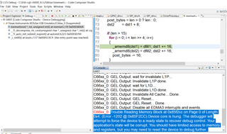
C66xx_0:
Trouble Reading Memory Block at 0x85f1ac on Page 0 of Length 0x4:
(Error -1202 @ 0x85F1AC) Device core is hung.
The debugger will attempt to force the device to a ready state to recover debug control.
Your application's state will be corrupt. You should have limited access to memory and registers,
but you may need to reset the device to debug further. (Emulation package 5.1.232.0)
This was the IDE UI's snapshot:

This occured every time I power up my board .
Could any experienced engineer give me some solving methods or possible clues for this malfunction ?
Thank you very much!!

  • Also: if I tried to load some data into 0xc000000 memory region,it always failed and display similar information as above just like "Trouble Reading Memory Block at 0xc000000 on Page 0 of Length 0x4...".It seemed that memory region in the DSP was not ready for access.

  • ,

    It is always good to start with something working.

    If you have the C6657 Ti-EVM, 

    Please follow the steps given in this FAQ for the " target connection" .

    https://e2e.ti.com/support/processors-group/processors/f/processors-forum/1057447/faq-tms320c6657-how-to-build-and-run-the-ipc-example-on-c6657-evm

    --

    For the custom board, you have to modify the gel file, "evmc6657l.gel" located at "\ti\ccs930\ccs\ccs_base\emulation\boards\evmc6657l\gel" 

    Regards

    Shankari G

  • Thank you very much for your reply!

    Yes, I have modified the gel file according to my custom board's configure and I have C6657 Ti-EVM in hand.
    The same gel file and programme can work well using C6657 Ti-EVM.
    Actually my custom board is based on C6657 Ti-EVM's design only eliminating some unused chips according to my application.
    In the gel file,related modification is made. 
    I have measured every key signals' timing sequence during the progress of  powering on without finding any possible errors according to C6657's datasheet and hardware design manual reference.

    The power on problem of my custom board is really frustrating me recently.

    Any assistants from you is highly appreciated!

  • Hi Zhongyuan,

    Yes, I have modified the gel file according to my custom board's configure and I have C6657 Ti-EVM in hand.

    Since you have modified the GEL file, Kindly do GEL file debugging, add GEL hardware breakpoints and make sure GEL grammar rules is maintained.

    Please refer to this URL for GEL file debugging, https://software-dl.ti.com/ccs/esd/documents/users_guide/ccs_debug-gel.html.

    It will help to isolate the issue to either hardware or software.

    Thanks

    Rajarajan U

  • Hi Zhongyuan,

    What is the DRAM chip used ? for your custom board.

    Accordingly,  the DDR3 register values have to be changed in the gel file.

    ---

    Please have a look at this FAQ on configuring the values of DDR3 registers.

    https://e2e.ti.com/support/processors-group/processors/f/processors-forum/1096375/faq-66ak2e05-how-to-calculate-the-ddr3-interface-registers-for-keystone-ii-devices-and-test-debug-on-keystone-ii-evm

    The above link is for Keystone - II devices. But the sequence is similar.

    For example, instead of "Keystone II DDR3 Initialization guide" , we have to go through the "Keystone I DDR3 Initialization guide" - https://www.ti.com/lit/an/sprabl2e/sprabl2e.pdf

    ---

    Rajan's suggestion of ---- running a hello world example ----  is possible only after a successful run of GEl file.

    As per your snapshot, the gel file was not successful, on the first hand.

    --

    On the second hand, please have a look at the XDS connection issues also.

    Jtag connectivity issues:

    ==================

    https://software-dl.ti.com/ccs/esd/documents/ccs_debugging_jtag_connectivity_issues.html

    https://dev.ti.com/tirex/explore/node?node=AOi9Jj0vmBMJ0KQKaKITgg__FUz-xrs__LATEST

    https://www.ti.com/lit/ug/spru641/spru641.pdf

    https://www.ti.com/lit/ug/spru655i/spru655i.pdf

    Regards

    Shankari G

  • Hi Zhongyuan,

    When I had a closer look to your Snapshot of the gel output,

    it seems to me,

    1. It throws error while validating the L1P and L1D memory.

    2. It is the error thrown from the GEl output and not from your application.

    3. Please post your gel output in text format instead of snapshot.

    ---

    The successful iniialization of gel sequence will be something like below on the C6657 board.

    Compare this output messages with yours.

    For example... focus on the portion where it setup the "cache". It throws invalidate cache on your snapshot.

     C66xx_0: GEL Output: Setup Cache...
    C66xx_0: GEL Output: L1P = 32K
    C66xx_0: GEL Output: L1D = 32K

    ====

    C66xx_0: GEL Output: Setup_Memory_Map...
    C66xx_0: GEL Output: Setup_Memory_Map... Done.
    C66xx_1: GEL Output: Setup_Memory_Map...
    C66xx_1: GEL Output: Setup_Memory_Map... Done.
    C66xx_0: GEL Output:
    Connecting Target...
    C66xx_0: GEL Output: DSP core #0
    C66xx_0: GEL Output: C6657L GEL file Ver is 1.00800002
    C66xx_0: GEL Output: Global Default Setup...
    C66xx_0: GEL Output: Setup Cache...
    C66xx_0: GEL Output: L1P = 32K
    C66xx_0: GEL Output: L1D = 32K
    C66xx_0: GEL Output: L2 = ALL SRAM
    C66xx_0: GEL Output: Setup Cache... Done.
    C66xx_0: GEL Output: Main PLL (PLL1) Setup ...
    C66xx_0: GEL Output: PLL in Bypass ...
    C66xx_0: GEL Output: pll_multiplier = (19)
    C66xx_0: GEL Output: PLL1_PLLM = (19)
    C66xx_0: GEL Output: PLL1_CMD = (1)
    C66xx_0: GEL Output: PLL1 Setup for DSP @ 1000.0 MHz.
    C66xx_0: GEL Output: SYSCLK2 = 333.333344 MHz, SYSCLK5 = 200.0 MHz.
    C66xx_0: GEL Output: SYSCLK8 = 15.625 MHz.
    C66xx_0: GEL Output: PLL1 Setup... Done.
    C66xx_0: GEL Output: Power on all PSC modules and DSP domains...
    C66xx_0: GEL Output: Power on all PSC modules and DSP domains... Done.
    C66xx_0: GEL Output: DDR3 PLL (PLL2) Setup ...
    C66xx_0: GEL Output: DDR3 PLL Setup... Done.
    C66xx_0: GEL Output: DDR3 Init begin (1333 auto)
    C66xx_0: GEL Output: XMC Setup ... Done
    C66xx_0: GEL Output: IFRDY bit is SET: DDR3 Interface Ready
    C66xx_0: GEL Output:
    DDR3 initialization is complete.
    C66xx_0: GEL Output: DDR3 Init done
    C66xx_0: GEL Output: DDR3 memory test... Started
    C66xx_0: GEL Output: DDR3 memory test... Passed
    C66xx_0: GEL Output: PLL and DDR3 Initialization completed(0) ...
    C66xx_0: GEL Output: configSGMIISerdes Setup... Begin
    C66xx_0: GEL Output: SGMII SERDES has been configured.
    C66xx_0: GEL Output: Enabling EDC ...
    C66xx_0: GEL Output: L1P error detection logic is enabled.
    C66xx_0: GEL Output: L2 error detection/correction logic is enabled.
    C66xx_0: GEL Output: MSMC error detection/correction logic is enabled.
    C66xx_0: GEL Output: Enabling EDC ...Done
    C66xx_0: GEL Output: Global Default Setup... Done.

    ===================

    Regards

    Shankari G