


Environment:
TMS320C6745 EDMA3 for uart1 RX
Dear all, please can you help me?
I'm try to view the cache memory in CCS12 :
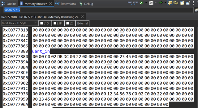
What is the difference of marking the L1D, L1P and L2 fields? In the above view I can see the content when I stop the debugger.
If I run the debugger I see
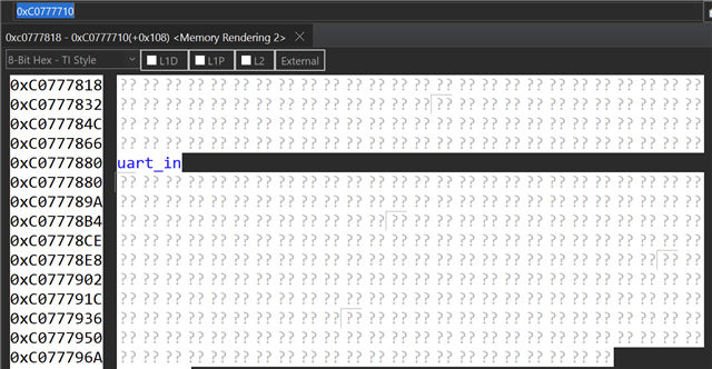
When I marked L1D and L2 I see only 00 fields.
The reason for all is that I program the EDMA3 for the uart1 and I want to see every time I got new data in the uart I will display it
immediate in the memory browser. Is this possible?
Do I things wrong withe the memory controller
#define CACHE_DMA_NULL 0x00000000
#define CACHE_DMA_L2WB 0x00000001
#define CACHE_DMA_L2WBINV 0x00000002
#define CACHE_DMA_L2INV 0x00000004
#define CACHE_DMA_L2WWC 0x00000010
#define CACHE_DMA_L2WIWC 0x00000020
#define CACHE_DMA_L2IWC 0x00000040
I used only L2WWC. Where can I find an explanation on how to use the DMA programming?
I red a the document SPRUFK5A mega module, but it is not clear for me. Do you have an example for the EDMA3 uart?
Best regards
Martin
