Part Number: TDA4VM
Other Parts Discussed in Thread: DRA821,
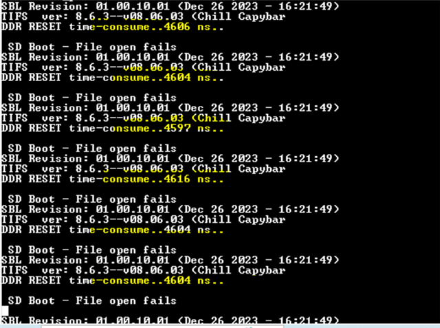
In the offline hardware testing of the factory, there is a problem of TDA4 DDR initialization failure,
especially in the case of repeated warm resets on a single ECU with a higher probability.
by debug, the software enters a while loop at Board_DDRInit function.
We used hynix's DDR H54G56BYYPX046(4G)
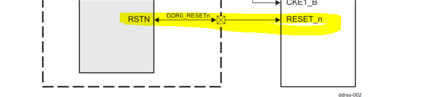
Please analyze the reasons based on the following two cases and determine if it is necessary to modify board_ddrRegInit.h? See attachment.
case1:
Board_DDRChangeFreqAck
while(regVal == 0x0)
{
regVal = HW_RD_REG32(BOARD_DDR_FSP_CLKCHNG_REQ_ADDR) & 0x80;
BOARD_DEBUG_LOG("Reg Value: %d \n", regVal);
}
case2:
LPDDR4_PollPhyIndepIrq
LPDDR4_CheckPhyIndepInterrupt
/* Loop until irqStatus found to be 1 or if value of 'result' !=CDN_EOK */
do {
if (++timeout == delay) {
result = CDN_EIO;
break;
}
CPS_DelayNs(10000000U);
result = LPDDR4_CheckPhyIndepInterrupt(pD, irqBit, &irqStatus);
} while ((irqStatus == false) && (result == (uint32_t)CDN_EOK));