Hello TI expert,
Regarding the safety mechanism of DDR9 write/read, we have some questions with how to realize it:
We know that the SM could be realized eith at Main domain A core or at MCU domain, and it can be executed at boot or peridically.
Our design configuration: 4 pcs 2G DDR, and now we set the monitor size of 64*1024bit for each piece DDR.
Question1: If we the SM is realized at Main domain, in order to achive a high diagnosis coverage, how many size space should be monitored according to your experience? And if you have any suggestions for the selected address area?
Question2: If we the SM is realized at MCU domain, in order to achive a high diagnosis coverage, how many size space should be monitored according to your experience? And if you have any suggestions for the selected address area?
Question3: we learned that the DDR9 is worked at interleaver model, when one fault is qulified, we don't know which piece DDR of the fault was from, my I ask is it sure? If yes, do you have any measure to solve this issue?
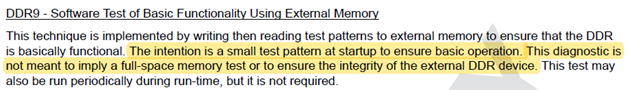
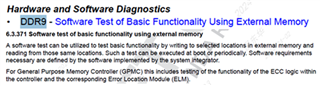
FYI: the sreenshort of DDR9 from safety manual.
Thanks in advance.