This thread has been locked.

If you have a related question, please click the "Ask a related question" button in the top right corner. The newly created question will be automatically linked to this question.

AM625: AM6254 gpmc for nand ,sram and FPGA

Part Number: AM625
Other Parts Discussed in Thread: SK-AM62, AM5718, AM3354

HI,

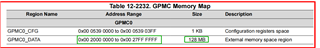
I have the problem on the GPMC interface. for hardware ,we have set cs0 for NAND (8 bit  A/D multiplexed mode). cs2 for 256K sram (18bit ad lines ,16 bit D lines).
cs3 for 1M FPGA (20 bit AD lines ,16bit D lines).so how to cofigure GPMC in the dts ? 
 just configure the GPMC for NAND, the nand works oK . 
 so we want to know how to configure sram and fpga at the same time .
 hope your advices as soon as possible .

Thanks !

  • Hello Helen Han,

    I assume that you are using A53 core for all the above interfaces, and can you please confirm ?

    https://e2e.ti.com/support/processors-group/processors/f/processors-forum/1349234/faq-am24x-am64x-am62x-what-are-the-maximum-sizes-of-nand-or-nor-or-psram-memories-that-can-be-connected-to-gpmc-for-the-am24x-am64x-am62x

    Can you please look at the link above about how much sizes can be connected to Am6x devices ?

    We don't recommend to connect all devices on connectivity which will increase bus capacitances and may result in GPMc malfunction.

    Regards,

    Anil.

  • Hi Swargam Anil,
    AM6254 :NAND,SRAM ,FPGA are all connect to A53 core interface.

    NAND :cs0, 8bit  Address and data multiplexed, 1G Byte.
    SRAM:cs2,16 bit Address and data None Multiplexed ,256k *16bit = 512K byte
    FPGA:cs3,16BIT Address and data None Multiplexed ,256K*16bit = 512K byte.

  • I  have configure the nand and sram  in the dts . 

    &gpmc0 {
    status = "okay";
    pinctrl-names = "default";
    pinctrl-0 = <&gpmc0_pins_default>;
    ranges = <0 0 0x0 0x51000000 0x01000000>; /* CS0 space. Min partition = 16MB */
    ranges = <2 0 0x0 0x52000000 0x40000>; /* CS2 space. Min partition = 4MB */
    #address-cells = <2>;
    #size-cells = <1>;

    nand@0,0 {
    compatible = "ti,am64-nand";
    reg = <0 0 64>; /* device IO registers */
    interrupt-parent = <&gpmc0>;
    interrupts = <0 IRQ_TYPE_NONE>, /* fifoevent */
    <1 IRQ_TYPE_NONE>; /* termcount */
    rb-gpios = <&gpmc0 0 GPIO_ACTIVE_HIGH>; /* gpmc_wait0 */
    ti,nand-xfer-type = "prefetch-polled";
    ti,nand-ecc-opt = "bch8"; /* BCH8: Bootrom limitation */
    ti,elm-id = <&elm0>;
    nand-bus-width = <8>;
    gpmc,device-width = <1>;
    gpmc,sync-clk-ps = <0>;
    gpmc,cs-on-ns = <0>;
    gpmc,cs-rd-off-ns = <40>;
    gpmc,cs-wr-off-ns = <40>;
    gpmc,adv-on-ns = <0>;
    gpmc,adv-rd-off-ns = <25>;
    gpmc,adv-wr-off-ns = <25>;
    gpmc,we-on-ns = <0>;
    gpmc,we-off-ns = <20>;
    gpmc,oe-on-ns = <3>;
    gpmc,oe-off-ns = <30>;
    gpmc,access-ns = <30>;
    gpmc,rd-cycle-ns = <40>;
    gpmc,wr-cycle-ns = <40>;
    gpmc,bus-turnaround-ns = <0>;
    gpmc,cycle2cycle-delay-ns = <0>;
    gpmc,clk-activation-ns = <0>;
    gpmc,wr-access-ns = <40>;
    gpmc,wr-data-mux-bus-ns = <0>;

    partitions {
    compatible = "fixed-partitions";
    #address-cells = <1>;
    #size-cells = <1>;

    partition@0 {
    label = "NAND.tiboot3";
    reg = <0x00000000 0x00200000>; /* 2M byte*/
    };
    partition@200000 {
    label = "NAND.tispl";
    reg = <0x00200000 0x00200000>; /* 2M */
    };
    partition@400000 {
    label = "NAND.u-boot";
    reg = <0x00400000 0x00400000>; /* 4M */
    };
    partition@800000 {
    label = "NAND.u-boot-env";
    reg = <0x00800000 0x00100000>; /* 1M */
    };
    partition@900000 {
    label = "NAND.file-system";
    reg = <0x00900000 0x31600000>; /* 790M */
    };
    };
    };

    sram@2,0 {
    //compatible = "ti,am64-nand";
    reg = <2 0 64>; /* device IO registers */
    nand-bus-width = <16>;
    gpmc,device-width = <2>;
    gpmc,sync-clk-ps = <0>;
    gpmc,cs-on-ns = <0>;
    gpmc,cs-rd-off-ns = <40>;
    gpmc,cs-wr-off-ns = <40>;
    gpmc,adv-on-ns = <0>;
    gpmc,adv-rd-off-ns = <35>;
    gpmc,adv-wr-off-ns = <35>;
    gpmc,we-on-ns = <0>;
    gpmc,we-off-ns = <50>;
    gpmc,oe-on-ns = <3>;
    gpmc,oe-off-ns = <30>;
    gpmc,access-ns = <50>;
    gpmc,rd-cycle-ns = <60>;
    gpmc,wr-cycle-ns = <60>;
    gpmc,bus-turnaround-ns = <0>;
    gpmc,cycle2cycle-delay-ns = <0>;
    gpmc,clk-activation-ns = <0>;
    gpmc,wr-access-ns = <40>;
    gpmc,wr-data-mux-bus-ns = <0>;
    };

    };


    when kernel runing . I got the information:
    [ 1.100486] gpmc_mem_init: disabling cs 0 mapped at 0x0-0x1000000
    [ 1.107158] omap-gpmc 3b000000.memory-controller: /bus@f0000/memory-controller@3b000000/nand@0,0 has malformed 'reg' property
    [ 1.118748] omap-gpmc 3b000000.memory-controller: failed to probe DT child 'nand': -19

    but I just add rangs and sram node in the GPMC . why the nand  node has malformed "reg"property.
    so what's the problem in the gpmc configure in the dts?
     and how to confirm the sram works ?

  • Hello Helen Han,

    NAND :cs0, 8bit  Address and data multiplexed, 1G Byte.

    In your project there are problems with the size configurations.

    For NAND memories there are no issues with size limitations.

    But for CS2 and CS3 you have configured 512K bytes, which is not supported by AM62X., In this 16bit not multiplexed, you can connect maximum 8M bytes for NOR and PSRAM .

    One more thing is that when you connect different memories on the same GPMC bus, which increases the bus capacitance which will create the malfunction of GPMC peripheral and to overcome these issues you need have proper pcb routing and will operate GPMC clock at lower frequencies.

    Please look at the FAQ below for more details about how much sizes can be connected to AM62x.

    https://e2e.ti.com/support/processors-group/processors/f/processors-forum/1349234/faq-am24x-am64x-am62x-what-are-the-maximum-sizes-of-nand-or-nor-or-psram-memories-that-can-be-connected-to-gpmc-for-the-am24x-am64x-am62x

    but I just add rangs and sram node in the GPMC . why the nand  node has malformed "reg"property.
    so what's the problem in the gpmc configure in the dts?
     and how to confirm the sram works ?

    I am not the right person to comment on this issue and routing your query to Linux expert to comment on above issue.

    Regards,

    Anil.

  • Hi, Anil.

    But for CS2 and CS3 you have configured 512K bytes, which is not supported by AM62X., In this 16bit not multiplexed, you can connect maximum 8M bytes for NOR and PSRAM .

    what does this mean? the CS2 configured 512K , CS3 configured 512K . the total of CS2 and CS3 is 1M bytes. it is more minimum than 8M for NOR and PSRAM.
     I am sorry that i didn’t understand that it is not supported by AM62X.

  • Hello Anil,
     I found some information in the datasheet(AM62x Processors Silicon Revision 1.0 Texas Instruments Families of Products).
     1.in chapter 2 of memory map ,page 43

    2.in chapter General-Purpose Memory Controller(GPMC) ,page10012


    why the GPMC0_DATA has different regions?

  • Hi Helen,

    2.in chapter General-Purpose Memory Controller(GPMC) ,page10012

    Are you referring to the latest version of the TRM?

    I don't see this Table 12-2232 exists in TRM revB.

  • HI, TRM‘s version is 

    SPRUIV7A – MAY 2022 – REVISED NOVEMBER 2022. I will update to the lastest version.

    but the question is how to use the nand and sram in the GPMC.

  • Hi  Swargam Anil,
     I found some information in ti-aemif.txt in kernel document . 
    does the sram  support by compatible "ti,davinci-aemif"?
    I am urgent with the GPMC to connect the sram function .
    could you give me some advices or guides  how to achieve it ?

  • Hi Swargam Anil,
     does am6254 support sram device by GPMC ?
    I checked all the linux source code , I didn't find some information about it .

    do you give some helps ?

  • Hi Helen,

     I found some information in ti-aemif.txt in kernel document . 
    does the sram  support by compatible "ti,davinci-aemif"?

    No, the davinci-aemif is a different hardware module, and it uses a different kernel driver which AM62x GPMC uses.

     does am6254 support sram device by GPMC ?

    The AM62x TRM Section 12.4.3.1 GPMC Overwiew does say it supports Pseudo-SRAM device.

    The SK-AM62 EVM doesn't use the GPMC interface, so I am unable to directly tell your configuration for NAND/SRAM/FPGA is correct or not. But I recommend to do the following:

    - enable one device / GPMC CSx at a time;

    - compare the NAND/SRAM/FPGA device datasheet and directly configure the GPMC registers GPMC_CONFIGx to ensure the device works, then convert the GPMC_CONFIGx register settings to kernel device tree.

  • HI,I have confirmed the registers GPMC_CS_CONFIG0~GPMC_CS_CONFIG7, the configure is right.
    the gpmc ranges configure below:

    ranges = <0 0 0x0 0x52000000 0x01000000>, /* CS0 space. Min partition = 16MB */  //nand
    <2 0 0x0 0x51000000 0x01000000>; /* CS2 space. Min partition = 4MB */  //sram

    but after the system boot from nand , I use devmem2 command , I get the information like this:
    root@am62xx-evm:~# devmem2 0x52000000
    /dev/mem opened.
    Memory mapped at address 0xffffb586f000.
    Read at address 0x52000000 (0xffffb586f000): 0xFFFFFFFF
    root@am62xx-evm:~# devmem2 0x51000000
    /dev/mem opened.
    Memory mapped at address 0xffffba705000.
    Read at address 0x51000000 (0xffffba705000): 0x84CD34CC
    root@am62xx-evm:~#

    the 0x51000000 is the base address of sram , but it has values.
    but 0x52000000 is the base address of nand , the value is 0xffffffff. 

    the system is boot from nand .

    why the value is so strange?

  • Hi Helen,

    I am confused, you can boot from nand, but have issue in device tree config for nand? How have you flashed the boot image to nand?

    root@am62xx-evm:~# devmem2 0x51000000
    /dev/mem opened.
    Memory mapped at address 0xffffba705000.
    Read at address 0x51000000 (0xffffba705000): 0x84CD34CC

    It is normal that SRAM shows random data after power on.

    root@am62xx-evm:~# devmem2 0x52000000
    /dev/mem opened.
    Memory mapped at address 0xffffb586f000.
    Read at address 0x52000000 (0xffffb586f000): 0xFFFFFFFF

    The NAND flash seems no data have been written to.

  • Hi Bin,
     I flash boot image to nand after the system boot from sd card.

    I have do some tests:

    1、just cofigure nand in the dts.

    ranges = <0 0 0x0 0x52000000  0x01000000>;

    nand@0,0 {
    compatible = "ti,am64-nand";
    reg = <0 0 64>; /* device IO registers */

    ....

    use devmem2 command . devmem2 0x52000000  ,the value is 0xFFFFFFFF.

    use cat /proc/iomem,the result is:


     52000000-5200003f : 52000000.nand nand@0,0

    use nanddump command, I get /dev/mtd0 to files.  compiled the read files and files which flash to nand, the two files are equals.

    2、cofigure nand and sram in the dts.

    ranges = <0 0 0x0 0x52000000 0x01000000>, /* CS0 space. Min partition = 16MB */
    <2 0 0x0 0x51000000 0x01000000>; /* CS2 space. Min partition = 4MB */

    use cat /proc/iomem:

    there is only nand informaiton ,there is no sram information .

    52000000-5200003f : 52000000.nand nand@0,0

    use devmem2 command . devmem2 0x5200000, the value is 0xFFFFFFF.

    root@am62xx-evm:~# devmem2 0x51000000
    /dev/mem opened.
    Memory mapped at address 0xffffb54f1000.
    Read at address 0x51000000 (0xffffb54f1000): 0x84CD34CC
    root@am62xx-evm:~# devmem2 0x52000000

    but the problem is the value of address 0x51000000 is the same  after system starts everytime .

     it is not a random vlaue .

    so the problem is after I configure in the dts of cs0 range and cs2 range. 
    I can use devmem2 cmd to read the two range address.

    but the value seems not  read from externel devices . why ?

    this is my first time to use GPMC, I am not formiliar it . is there something  wrong  understand with it ?
    or do I need to add the kernel driver to achieve gpmc to control sram?


  • Hi Bin,

    now I use nandump cmd to read data from nand , I use oscilloscope to catch GPMC_CS0, the cs0 signal is  low in data tranmit.

    but when I use devmem2 0x52000000, the cs signal has no change , it is always high .

    so why devmem2 read phyical address didn't reach the nand device ?

    then whether I can doubt that the sram didn't work in the last response ?

  • Hi Bin ,
    the GPMC configure in the dts:

    gpmc0_pins_default: gpmc0-pins-default {
    pinctrl-single,pins = <
    AM62X_IOPAD(0x00b8, PIN_OUTPUT, 1) /* (U22) VOUT0_DATA0.GPMC0_A0 */
    AM62X_IOPAD(0x00bc, PIN_OUTPUT, 1) /* (V24) VOUT0_DATA1.GPMC0_A1 */
    AM62X_IOPAD(0x00e0, PIN_OUTPUT, 1) /* (V20) VOUT0_DATA10.GPMC0_A10 */
    AM62X_IOPAD(0x00e4, PIN_OUTPUT, 1) /* (AA23) VOUT0_DATA11.GPMC0_A11 */
    AM62X_IOPAD(0x00e8, PIN_OUTPUT, 1) /* (AB25) VOUT0_DATA12.GPMC0_A12 */
    AM62X_IOPAD(0x00ec, PIN_OUTPUT, 1) /* (AA24) VOUT0_DATA13.GPMC0_A13 */
    AM62X_IOPAD(0x00f0, PIN_OUTPUT, 1) /* (Y22) VOUT0_DATA14.GPMC0_A14 */
    AM62X_IOPAD(0x00f4, PIN_OUTPUT, 1) /* (AA21) VOUT0_DATA15.GPMC0_A15 */
    AM62X_IOPAD(0x00f8, PIN_OUTPUT, 1) /* (AB24) VOUT0_HSYNC.GPMC0_A16 */
    AM62X_IOPAD(0x00fc, PIN_OUTPUT, 1) /* (Y20) VOUT0_DE.GPMC0_A17 */
    AM62X_IOPAD(0x0100, PIN_OUTPUT, 1) /* (AC25) VOUT0_VSYNC.GPMC0_A18 */
    AM62X_IOPAD(0x0104, PIN_OUTPUT, 1) /* (AC24) VOUT0_PCLK.GPMC0_A19 */
    AM62X_IOPAD(0x00c0, PIN_OUTPUT, 1) /* (W25) VOUT0_DATA2.GPMC0_A2 */
    AM62X_IOPAD(0x00c4, PIN_OUTPUT, 1) /* (W24) VOUT0_DATA3.GPMC0_A3 */
    AM62X_IOPAD(0x00c8, PIN_OUTPUT, 1) /* (Y25) VOUT0_DATA4.GPMC0_A4 */
    AM62X_IOPAD(0x00cc, PIN_OUTPUT, 1) /* (Y24) VOUT0_DATA5.GPMC0_A5 */
    AM62X_IOPAD(0x00d0, PIN_OUTPUT, 1) /* (Y23) VOUT0_DATA6.GPMC0_A6 */
    AM62X_IOPAD(0x00d4, PIN_OUTPUT, 1) /* (AA25) VOUT0_DATA7.GPMC0_A7 */
    AM62X_IOPAD(0x00d8, PIN_OUTPUT, 1) /* (V21) VOUT0_DATA8.GPMC0_A8 */
    AM62X_IOPAD(0x00dc, PIN_OUTPUT, 1) /* (W21) VOUT0_DATA9.GPMC0_A9 */
    AM62X_IOPAD(0x003c, PIN_INPUT, 0) /* (M25) GPMC0_AD0 */
    AM62X_IOPAD(0x0040, PIN_INPUT, 0) /* (N23) GPMC0_AD1 */
    AM62X_IOPAD(0x0064, PIN_INPUT, 0) /* (T25) GPMC0_AD10 */
    AM62X_IOPAD(0x0068, PIN_INPUT, 0) /* (R21) GPMC0_AD11 */
    AM62X_IOPAD(0x006c, PIN_INPUT, 0) /* (T22) GPMC0_AD12 */
    AM62X_IOPAD(0x0070, PIN_INPUT, 0) /* (T24) GPMC0_AD13 */
    AM62X_IOPAD(0x0074, PIN_INPUT, 0) /* (U25) GPMC0_AD14 */
    AM62X_IOPAD(0x0078, PIN_INPUT, 0) /* (U24) GPMC0_AD15 */
    AM62X_IOPAD(0x0044, PIN_INPUT, 0) /* (N24) GPMC0_AD2 */
    AM62X_IOPAD(0x0048, PIN_INPUT, 0) /* (N25) GPMC0_AD3 */
    AM62X_IOPAD(0x004c, PIN_INPUT, 0) /* (P24) GPMC0_AD4 */
    AM62X_IOPAD(0x0050, PIN_INPUT, 0) /* (P22) GPMC0_AD5 */
    AM62X_IOPAD(0x0054, PIN_INPUT, 0) /* (P21) GPMC0_AD6 */
    AM62X_IOPAD(0x0058, PIN_INPUT, 0) /* (R23) GPMC0_AD7 */
    AM62X_IOPAD(0x005c, PIN_INPUT, 0) /* (R24) GPMC0_AD8 */
    AM62X_IOPAD(0x0060, PIN_INPUT, 0) /* (R25) GPMC0_AD9 */
    AM62X_IOPAD(0x0098, PIN_INPUT, 0) /* (U23) GPMC0_WAIT0 */
    AM62X_IOPAD(0x009c, PIN_INPUT, 0) /* (V25) GPMC0_WAIT1 */
    AM62X_IOPAD(0x0094, PIN_OUTPUT, 0) /* (N20) GPMC0_BE1n */
    AM62X_IOPAD(0x00a8, PIN_OUTPUT_PULLUP, 0) /* (M21) GPMC0_CSn0 */
    AM62X_IOPAD(0x00ac, PIN_OUTPUT_PULLUP, 0) /* (L21) GPMC0_CSn1 */
    AM62X_IOPAD(0x00b0, PIN_OUTPUT_PULLUP, 0) /* (K22) GPMC0_CSn2 */
    AM62X_IOPAD(0x00b4, PIN_OUTPUT_PULLUP, 0) /* (K24) GPMC0_CSn3 */
    AM62X_IOPAD(0x007c, PIN_OUTPUT, 0) /* (P25) GPMC0_CLK */
    AM62X_IOPAD(0x0084, PIN_OUTPUT, 0) /* (L23) GPMC0_ADVn_ALE */
    AM62X_IOPAD(0x0088, PIN_OUTPUT_PULLUP, 0) /* (L24) GPMC0_OEn_REn */
    AM62X_IOPAD(0x008c, PIN_OUTPUT_PULLUP, 0) /* (L25) GPMC0_WEn */
    AM62X_IOPAD(0x0090, PIN_OUTPUT, 0) /* (M24) GPMC0_BE0n_CLE */
    AM62X_IOPAD(0x00a0, PIN_OUTPUT_PULLUP, 0) /* (K25) GPMC0_WPn */
    AM62X_IOPAD(0x00a4, PIN_OUTPUT, 0) /* (M22) GPMC0_DIR */
    >;
    };

    };

    &gpmc0 {
    status = "okay";
    pinctrl-names = "default";
    pinctrl-0 = <&gpmc0_pins_default>;
    ranges = <0 0 0x0 0x52000000 0x01000000>, /* CS0 space. Min partition = 16MB */
    <2 0 0x0 0x51000000 0x01000000>; /* CS2 space. Min partition = 4MB */
    #address-cells = <2>;
    #size-cells = <1>;

    nand@0,0 {
    compatible = "ti,am64-nand";
    reg = <0 0 64>; /* device IO registers */
    interrupt-parent = <&gpmc0>;
    interrupts = <0 IRQ_TYPE_NONE>, /* fifoevent */
    <1 IRQ_TYPE_NONE>; /* termcount */
    rb-gpios = <&gpmc0 0 GPIO_ACTIVE_HIGH>; /* gpmc_wait0 */
    ti,nand-xfer-type = "prefetch-polled";
    ti,nand-ecc-opt = "bch8"; /* BCH8: Bootrom limitation */
    ti,elm-id = <&elm0>;
    nand-bus-width = <8>;
    gpmc,device-width = <1>;
    gpmc,sync-clk-ps = <0>;
    gpmc,cs-on-ns = <0>;
    gpmc,cs-rd-off-ns = <40>;
    gpmc,cs-wr-off-ns = <40>;
    gpmc,adv-on-ns = <0>;
    gpmc,adv-rd-off-ns = <25>;
    gpmc,adv-wr-off-ns = <25>;
    gpmc,we-on-ns = <0>;
    gpmc,we-off-ns = <20>;
    gpmc,oe-on-ns = <3>;
    gpmc,oe-off-ns = <30>;
    gpmc,access-ns = <30>;
    gpmc,rd-cycle-ns = <40>;
    gpmc,wr-cycle-ns = <40>;
    gpmc,bus-turnaround-ns = <0>;
    gpmc,cycle2cycle-delay-ns = <0>;
    gpmc,clk-activation-ns = <0>;
    gpmc,wr-access-ns = <40>;
    gpmc,wr-data-mux-bus-ns = <0>;

    partitions {
    compatible = "fixed-partitions";
    #address-cells = <1>;
    #size-cells = <1>;

    partition@0 {
    label = "NAND.tiboot3";
    reg = <0x00000000 0x00200000>; /* 2M byte*/
    };
    partition@200000 {
    label = "NAND.tispl";
    reg = <0x00200000 0x00200000>; /* 2M */
    };
    partition@400000 {
    label = "NAND.u-boot";
    reg = <0x00400000 0x00400000>; /* 4M */
    };
    partition@800000 {
    label = "NAND.u-boot-env";
    reg = <0x00800000 0x00100000>; /* 1M */
    };
    partition@900000 {
    label = "NAND.file-system";
    reg = <0x00900000 0x31600000>; /* 790M */
    };
    };
    };

    sram@2,0 {
    compatible = "ti,fram";
    phy_base = <0x51000000>;
    max_size = <0x40000>;
    #address-cells = <1>;
    #size-cells = <1>;
    reg = <2 0 64>; /* device IO registers */
    //reg = <2 0 0x40000>; /* device IO registers */
    nand-bus-width = <16>;
    gpmc,device-width = <2>;
    gpmc,sync-clk-ps = <2000>;
    gpmc,cs-on-ns = <0>;
    gpmc,cs-rd-off-ns = <200>;
    gpmc,cs-wr-off-ns = <200>;
    gpmc,adv-on-ns = <0>;
    gpmc,adv-rd-off-ns = <35>;
    gpmc,adv-wr-off-ns = <35>;
    gpmc,we-on-ns = <20>;
    gpmc,we-off-ns = <40>;
    gpmc,oe-on-ns = <20>;
    gpmc,oe-off-ns = <100>;
    gpmc,access-ns = <80>;
    gpmc,rd-cycle-ns = <120>;
    gpmc,wr-cycle-ns = <60>;
    gpmc,bus-turnaround-ns = <40>;
    gpmc,cycle2cycle-delay-ns = <20>;
    gpmc,clk-activation-ns = <0>;
    gpmc,wr-access-ns = <40>;
    gpmc,wr-data-mux-bus-ns = <20>;
    };
    };

    just for reference. but the  reg = <0 0 64>; /* device IO registers */ , what's meaning of erery part?

  • Is there someone give me some advices ?
     1/configure the nand and sram under GPMC. the /proc/iomem is only nand information ,no sram .

    2/devmem2 cmd can read nand cs0 and sram cs2 space ,but the value is 0xFFFFFFFF of nand , the vlaue is a constant vlaue of sram .

      and the cs0 and cs2 didn't change in cmd devmem2?

  • Hi Helen,

     I flash boot image to nand after the system boot from sd card.

    Since you can flash the NAND in Linux from SD card boot and boot from NAND also works, I think your NAND is configured properly.

    use nanddump command, I get /dev/mtd0 to files.  compiled the read files and files which flash to nand, the two files are equals.

    Yes, this means the NAND is flashed correctly.

    use devmem2 command . devmem2 0x52000000  ,the value is 0xFFFFFFFF.

    I am not sure this is a validate test. The NAND device is managed as MTD device in Linux, I don't think you should use devmem2 directly access NAND raw address.

    but the problem is the value of address 0x51000000 is the same  after system starts everytime .

    Can you please try to use devmem2 to modify this address to a different value, then power cycle the board  to see what the value of this address is? When power cycle the board, please remove the power supply completely to ensure the SRAM is fully discharged.

  • Hi Bin,
    I have test with devmem2 0x51000000 ,write a different value to it . then power cycle the board ,then see the value of 0x51000000 has changed. 
    but the problem is  cat /proc/iomem , there is no sram information of 0x51000000.

    and also ,when I use devmem2 cmd , I didn't see the cs2 signal change . so  how to make sure the 0x51000000 is the address of externel sram address?

  • HI Bin ,
     I use devmem2 cmd to read and write cs2  of start address 0x51000000, the cs2 signal is did't change and always high . so I think the data is not read from external devices sram. 
    the sram is powered both by the battay and system power., it is used to save some values before the system powered off.
    so the firsttime I write a value in the 0x51000000. then poweroff the system . 
    atfter the system is completely powerdoff.  I poweron the system .
    I use the devmem2 read 0x51000000. the value is not same with last power off.so I think I didn't write vlaue to external device sram.

    so the problem is where the vlaue from? it is very confused me .

  • Hi Helen,

    None of our EVM has a GPMC SRAM, so I don't have experience with it. Can you please remove the CS0 NAND related DTS node so that we can focus on SRAM configuration itself?

  • Hi Bin,
    okay。 I will remove the cs0  nand from dts . 
    but what can I do to test  SRAM ?

  • Hi Bin,
    today I test the hardware of CS signal . I configure cs2 as a gpio . then write 0 , I catch low level . 

    when write 1 , I catch high level. so the hardware of cs2 signal works ok .

    but configure cs2 to GPMC mode .  when run devmem2 cmd ,the cs2 is always high level. 

    so I am sure that gpmc didn't  set cs2 low level when read the cs2 space address.

    so how to solve this problem ?

  • HI,For the GPMC to sram , do you have some progress?

    for the gpmc driver, how to make cs2 to work?

  • Hi Helen,

    For testing, can you route GPMC CS0 pin to SRAM and modify DTS to use CS0 for SRAM to see if CS0 can work properly on SRAM?

  • HI Bin ,
     I have discussed with hardware designer , he tell me that it couldn't rout GPMC CS0 to sram .so  could  you provide other way to test?

  • Hi Helen,

    Can you just short CS0 and CS2 signals together in anywhere on the board?

  • Hi Bin ,

    I have confirmed the short CS0 and CS2 signal together with haradware designer, he think it could't do it , and he think it risk our harware board. so this way didn't work . 

  • Hi Helen,

    Do you mean the hardware designer doesn't want to short CS0 and CS2 to risk the board? or CS0 and CS2 are no accessible on your board to be shorted with a blue wire?

    I will ask our GPMC hardware expert to understand if there is a rick to short CS0 and CS2 signals.

  • Hi Bin,

    we have rount cs0 to sram . when use cmd devmem2 0x510000000(cs0 space ,0x510000000 for sram). the cs0 signal didn't change , it is always high level.
     we use cat /proc/iomem. there is no information about GPMC of sram .

  • Hi Bin ,

    do you have some progress? and how to do next ?

  • Hi Bin ,

    if I short CS0 to CS2, when I just config cs0 to NAND , the system can't find nand device .

  • Hi Helen,

    if I short CS0 to CS2, when I just config cs0 to NAND , the system can't find nand device .

    Okay, it seems shorting CS0 and CS2 is not a good debug idea. The CS pins might have a stronger pullup which prevents the active CS to go low.

    Anyway, as Anil commented at the beginning:

    We don't recommend to connect all devices on connectivity which will increase bus capacitances and may result in GPMc malfunction.

    connecting 3 different devices to GPMC is not recommended, and likely it won't function correctly. So even if we could properly configure the SRAM device, you still would have runtime issues with 3 GPMC devices.

  • Hi Bin,

    GPMC connect 3 different devices , it is informed by the TI hardware engineer. the link is https://e2e.ti.com/support/processors-group/processors/f/processors-forum/1237469/am625-the-gpmc-issue-for-am6254.

    I have found some information about the use GPMC to connect NAND,SRAM,FPGA, the application is on AM3364 and AM5718.

    AM3354 applcation link:https://e2e.ti.com/support/processors-group/processors/f/processors-forum/315716/am335x-connecting-sram-and-nand-by-gpmc

    AM5718 application link:https://www.forlinx.com/article_view_339.html

    so we think AM6254 gpmc also support GPMC to nand and sram and maximum 4 devices. 

    now I am confused  what you said.

    We don't recommend to connect all devices on connectivity which will increase bus capacitances and may result in GPMc malfunction.

    connecting 3 different devices to GPMC is not recommended, and likely it won't function correctly. So even if we could properly configure the SRAM device, you still would have runtime issues with 3 GPMC devices.

    do I  misundestangding of GPMC?

  • A  very long thread. Would like to input some thought. 

    #1. The GPMC CSn is 16MB minimum granularity. although the SRAM, FPGA space is less then that, still can configure 16MB for each CSn.

    #2. NAND is a block device and in-direct accessible device, can't use devmem2 to access, when operate on NAND, it is operating on GPMC registers. NAND flash doesn't have address.

    #3. devmem2 can access SRAM, NOR flash. they are direct addressable device.

  • when I use devmem2 cmd , I didn't see the cs2 signal change . so  how to make sure the 0x51000000 is the address of externel sram address?

    Dump out GPMC registers with devmem2 to check if configured in right way.

  • Hi Tony,
    I have configure the CS2 register. 
    the value is below:

    Read at address 0x3B0000C0 (0xffff8400b0c0): 0x00001000
    Read at address 0x3B0000C4 (0xffffa87760c4): 0x00060600
    Read at address 0x3B0000C8 (0xffffbea460c8): 0x00050500
    Read at address 0x3B0000CC (0xffffaca1c0cc): 0x07000401
    Read at address 0x3B0000D0 (0xffffa541e0d0): 0x00070808
    Read at address 0x3B0000D4 (0xffff947de0d4): 0x86000000
    Read at address 0x3B0000D8 (0xffff953190d8): 0x00000F51
    Read at address 0x3B0000DC (0xffffabcc80dc): 0x7F766E3B
    Read at address 0x3B0000E0 (0xffff872ec0e0): 0x77B779C7
    Read at address 0x3B0000E4 (0xffffa467f0e4): 0x7CF3D960

    I have confirmed the GPMC_COFNIG1_2 and GPMC_CONFIG1_7, it is as sram and  space address start 0x51000000 .

    but what means of  0x3B0000DC 、0x3B0000e0、  0x3B0000E4 for sram?

  • Hi Helen,

    From upper registers dump, CS2 mapped to 0x5100 0000, 16bit, asynchronous NOR-Flash like, Nonmultiplexed device.

    Ignore the NAND registers, not related to SRAM.

    Refer below Figure to configure rest timing field, you should be able to access the SRAM start from 0x51000000 to 0x51000000+SRAM size now. 

  • HI, I have configured the timing register like this:

    sram@2,0 {
    compatible = "ti,fram";
    phy_base = <0x51000000>;
    max_size = <0x40000>;
    #address-cells = <1>;
    #size-cells = <1>;
    reg = <2 0 64>; /* device IO registers */
    //reg = <2 0 0x40000>; /* device IO registers */
    nand-bus-width = <16>;
    gpmc,device-width = <2>;
    gpmc,sync-clk-ps = <0>;
    gpmc,cs-on-ns = <0>;
    gpmc,cs-rd-off-ns = <85>;
    gpmc,cs-wr-off-ns = <90>;
    gpmc,adv-on-ns = <0>;
    gpmc,adv-rd-off-ns = <35>;
    gpmc,adv-wr-off-ns = <35>;
    gpmc,we-on-ns = <5>;
    gpmc,we-off-ns = <60>;
    gpmc,oe-on-ns = <10>;
    gpmc,oe-off-ns = <60>;
    gpmc,access-ns = <75>; //max75
    gpmc,rd-cycle-ns = <90>; //min =75ns max=90ns
    gpmc,wr-cycle-ns = <90>; //min65ns
    gpmc,bus-turnaround-ns = <0>;
    gpmc,cycle2cycle-delay-ns = <30>;
    gpmc,clk-activation-ns = <0>;
    gpmc,wr-access-ns = <40>;
    gpmc,wr-data-mux-bus-ns = <0>;
    };

    our sram is  IS62WV25616EBLL-45TL.

    FA05-A76L-0101-0016 存储器 ISSI IS62WV25616EBLL-45TLI.pdf

    then below is my test:

    root@am62xx-evm:/root# devmem2 0x51000000 w 0x123456
    /dev/mem opened.
    Memory mapped at address 0xffffaeee9000.
    Read at address 0x51000000 (0xffffaeee9000): 0xFFFEFFFE
    Write at address 0x51000000 (0xffffaeee9000): 0x00123456, readback 0x00123456
    root@am62xx-evm:/root# devmem2 0x51000004 w 0x11223344
    /dev/mem opened.
    Memory mapped at address 0xffff9eb81000.
    Read at address 0x51000004 (0xffff9eb81004): 0x00120012
    Write at address 0x51000004 (0xffff9eb81004): 0x11223344, readback 0x11223344
    root@am62xx-evm:/root# devmem2 0x51000008 w 0x55667788
    /dev/mem opened.
    Memory mapped at address 0xffff92462000.
    Read at address 0x51000008 (0xffff92462008): 0x11221122
    Write at address 0x51000008 (0xffff92462008): 0x55667788, readback 0x55667788
    root@am62xx-evm:/root# devmem2 0x5100000c w 0xaabbccdd
    /dev/mem opened.
    Memory mapped at address 0xffffa1588000.
    Read at address 0x5100000C (0xffffa158800c): 0x55665566
    Write at address 0x5100000C (0xffffa158800c): 0xAABBCCDD, readback 0xAABBCCDD
    root@am62xx-evm:/root# devmem2 0x51000000
    /dev/mem opened.
    Memory mapped at address 0xffff9abac000.
    Read at address 0x51000000 (0xffff9abac000): 0xAABBAABB
    root@am62xx-evm:/root# devmem2 0x51000004
    /dev/mem opened.
    Memory mapped at address 0xffffa9fae000.
    Read at address 0x51000004 (0xffffa9fae004): 0xAABBAABB

     the read value  is wired, and at the same time , the cs2 is always high .

  • Based on the parameter, we can get below timing or writing and reading. as ADV is not used in non mux mode, it should not matter, but better to decrease ADVWEOFFTIME, ADVRDOFFTIME. 

    As you configured 3 CS, dump out the rest 2 set of gpmc config 0-7 registers. and the two error registers to check if any error triggered. 

    the read value  is wired, and at the same time , the cs2 is always high

    Can other signal also be probed? Can see signal toggling on other signal?

  • HI,I have  decrease ADVWEOFFTIME, ADVRDOFFTIME value from 35 to 10 and increase we-on-ns and oe-on-ns to 20ns. 

    test the result not change. the cs2 is always high, I checked the oe and cs3 signal are always high.

     I aslo  read the 0x3B000044 and 0x3B000048 , the value are all 0x0.

    now the dts just configure cs0 for nand and cs2 for sram.

    so what should we do next ?

  • I think need to create a overlay dtso file to verify it on AM62-SK and  probe CSn and RD, WE on user expansion header.


  • HI Tony,

    we have no SK-evm hardware. so do you help to test on your AM62-SK?

  • Can you share me your dts file, maybe I can test it sometime next week early.

  • Hi Tony, 

    this is kernel dts :

    // SPDX-License-Identifier: GPL-2.0
    /*
     * AM625 SK: https://www.ti.com/lit/zip/sprr448
     *
     * Copyright (C) 2021-2022 Texas Instruments Incorporated - https://www.ti.com/
     */
    
    /dts-v1/;
    
    #include <dt-bindings/leds/common.h>
    #include <dt-bindings/gpio/gpio.h>
    #include <dt-bindings/input/input.h>
    //#include <dt-bindings/net/ti-dp83867.h>
    #include "k3-am625.dtsi"
    
    / {
    	compatible = "ti,am625-sk", "ti,am625";
    	model = "Texas Instruments AM625 SK";
    	
    	aliases {
    		#serial0 = &mcu_uart0;
    		#serial1 = &wkup_uart0;
    		serial2 = &main_uart0;
    		#mmc0 = &sdhci0;
    		mmc1 = &sdhci1;
    		#mmc2 = &sdhci2;
    		#spi0 = &ospi0;
    		ethernet0 = &cpsw_port1;
    		#ethernet1 = &cpsw_port2;
    		usb0 = &usb0;
    		#usb1 = &usb1;
    	};
    
    	
    	chosen {
    		#address-cells = <2>;
    		#size-cells = <2>;
    		ranges;
    
    		stdout-path = "serial2:115200n8";
    		bootargs = "console=ttyS2,115200n8 earlycon=ns16550a,mmio32,0x02800000";
    
    		framebuffer0: framebuffer@0 {
    			compatible = "simple-framebuffer";
    			power-domains = <&k3_pds 186 TI_SCI_PD_EXCLUSIVE>;
    			clocks = <&k3_clks 186 6>,
    				 <&k3_clks 186 0>,
    				 <&k3_clks 186 2>;
    			display = <&dss>;
    			reg = <0x00 0xff700000 0x00 0x008ca000>;
    			width = <1024>; //800 ,1024
    			height = <768>; //600 ,768
    			stride = <(1024 * 4)>;//800*4
    			format = "x8r8g8b8";
    		};
    	};
    
    	opp-table {
    		/* Add 1.4GHz OPP for am625-sk board. Requires VDD_CORE to be at 0.85V */
    		opp-1400000000 {
    			opp-hz = /bits/ 64 <1400000000>;
    			opp-supported-hw = <0x01 0x0004>;
    			clock-latency-ns = <6000000>;
    		};
    	};
    
    	memory@80000000 {
    		device_type = "memory";
    		/* 2G RAM */
    		//reg = <0x00000000 0x80000000 0x00000000 0x80000000>;//2G
    		reg = <0x00000000 0x80000000 0x00000000 0x40000000>;//1G
    		//reg = <0x00000000 0x80000000 0x00000000 0x20000000>;//512M
    
    	};
    	reserved-memory {
    		#address-cells = <2>;
    		#size-cells = <2>;
    		ranges;
    
    		ramoops@9c700000 {
    			compatible = "ramoops";
    			reg = <0x00 0x9c700000 0x00 0x00100000>;
    			record-size = <0x8000>;
    			console-size = <0x8000>;
    			ftrace-size = <0x00>;
    			pmsg-size = <0x8000>;
    		};
    
    		/* global cma region */
    		linux,cma {
    			compatible = "shared-dma-pool";
    			reusable;
    			size = <0x00 0x8000000>; //128M
    			linux,cma-default;
    		};
    
    		rtos_ipc_memory_region: ipc-memories@9c800000 {
    			compatible = "shared-dma-pool";
    			reg = <0x00 0x9c800000 0x00 0x00300000>;
    			no-map;
    		};
    
    		mcu_m4fss_dma_memory_region: m4f-dma-memory@9cb00000 {
    			compatible = "shared-dma-pool";
    			reg = <0x00 0x9cb00000 0x00 0x100000>;
    			no-map;
    		};
    
    		mcu_m4fss_memory_region: m4f-memory@9cc00000 {
    			compatible = "shared-dma-pool";
    			reg = <0x00 0x9cc00000 0x00 0xe00000>;
    			no-map;
    		};
    
    		wkup_r5fss0_core0_dma_memory_region: r5f-dma-memory@9da00000 {
    			compatible = "shared-dma-pool";
    			reg = <0x00 0x9da00000 0x00 0x00100000>;
    			no-map;
    		};
    
    		wkup_r5fss0_core0_memory_region: r5f-memory@9db00000 {
    			compatible = "shared-dma-pool";
    			reg = <0x00 0x9db00000 0x00 0x00c00000>;
    			no-map;
    		};
    
    		secure_tfa_ddr: tfa@9e780000 {
    			reg = <0x00 0x9e780000 0x00 0x80000>;
    			alignment = <0x1000>;
    			no-map;
    		};
    
    		secure_ddr: optee@9e800000 {
    			reg = <0x00 0x9e800000 0x00 0x01800000>; /* for OP-TEE */
    			alignment = <0x1000>;
    			no-map;
    		};
    
    		framebuffer: framebuffer@ff700000 {
    			reg = <0x00 0xff700000 0x00 0x008ca000>;
    			no-map;
    		};
    	};
    
    	vmain_pd: regulator-0 {
    		/* TPS65988 PD CONTROLLER OUTPUT */
    		compatible = "regulator-fixed";
    		regulator-name = "vmain_pd";
    		regulator-min-microvolt = <5000000>;
    		regulator-max-microvolt = <5000000>;
    		regulator-always-on;
    		regulator-boot-on;
    	};
    
    	vcc_5v0: regulator-1 {
    		/* Output of LM34936 */
    		compatible = "regulator-fixed";
    		regulator-name = "vcc_5v0";
    		regulator-min-microvolt = <5000000>;
    		regulator-max-microvolt = <5000000>;
    		vin-supply = <&vmain_pd>;
    		regulator-always-on;
    		regulator-boot-on;
    	};
    
    	vcc_3v3_sys: regulator-2 {
    		/* output of LM61460-Q1 */
    		compatible = "regulator-fixed";
    		regulator-name = "vcc_3v3_sys";
    		regulator-min-microvolt = <3300000>;
    		regulator-max-microvolt = <3300000>;
    		vin-supply = <&vmain_pd>;
    		regulator-always-on;
    		regulator-boot-on;
    	};
    
    	vdd_mmc1: regulator-3 {
    		/* TPS22918DBVR */
    		compatible = "regulator-fixed";
    		regulator-name = "vdd_mmc1";
    		regulator-min-microvolt = <3300000>;
    		regulator-max-microvolt = <3300000>;
    		regulator-boot-on;
    		enable-active-high;
    		vin-supply = <&vcc_3v3_sys>;
    		//gpio = <&exp1 3 GPIO_ACTIVE_HIGH>;
    	};
    
    	vdd_sd_dv: regulator-4 {
    		/* Output of TLV71033 */
    		compatible = "regulator-gpio";
    		regulator-name = "tlv71033";
    		pinctrl-names = "default";
    		//pinctrl-0 = <&vdd_sd_dv_pins_default>;
    		regulator-min-microvolt = <1800000>;
    		regulator-max-microvolt = <3300000>;
    		regulator-boot-on;
    		vin-supply = <&vcc_5v0>;
    		//gpios = <&main_gpio0 31 GPIO_ACTIVE_HIGH>;
    		states = <1800000 0x0>,
    			 <3300000 0x1>;
    	};
    
    	vcc_1v8: regulator-5 {
    		/* output of TPS6282518DMQ */
    		compatible = "regulator-fixed";
    		regulator-name = "vcc_1v8";
    		regulator-min-microvolt = <1800000>;
    		regulator-max-microvolt = <1800000>;
    		vin-supply = <&vcc_3v3_sys>;
    		regulator-always-on;
    		regulator-boot-on;
    	};
    
    	wlan_lten: regulator-6 {
    		compatible = "regulator-fixed";
    		regulator-name = "wlan_lten";
    		regulator-min-microvolt = <3300000>;
    		regulator-max-microvolt = <3300000>;
    		vin-supply = <&vcc_3v3_sys>;
    		//gpios = <&exp1 11 GPIO_ACTIVE_LOW>;
    	};
    
    	wlan_en: regulator-7 {
    		compatible = "regulator-fixed";
    		regulator-name = "wlan_en";
    		regulator-min-microvolt = <1800000>;
    		regulator-max-microvolt = <1800000>;
    		vin-supply = <&wlan_lten>;
    		enable-active-high;
    		//gpios = <&main_gpio0 71 GPIO_ACTIVE_HIGH>;
    		pinctrl-names = "default";
    		//pinctrl-0 = <&wlan_en_pins_default>;
    	};
    
    	vdd_core: regulator-8 {
    		/* output of TPS62826DMQ */
    		compatible = "regulator-fixed";
    		regulator-name = "vdd_core";
    		regulator-min-microvolt = <850000>;
    		regulator-max-microvolt = <850000>;
    		vin-supply = <&vcc_3v3_sys>;
    		regulator-always-on;
    		regulator-boot-on;
    	};
    	
    	leds {
    		compatible = "gpio-leds";
    		pinctrl-names = "default";
    		pinctrl-0 = <&usr_led_pins_default
    		     &seg_pins_default>;
    
    		led-0 {
    			label = "LVDS_SEL6_8";
    			gpios = <&main_gpio1 7 GPIO_ACTIVE_LOW>;  
    			linux,default-trigger = "default-on";
    			default-state = "on";
    		};
    		
    		led-1 {
    			label = "LDVS_REV";
    			gpios = <&main_gpio1 8 GPIO_ACTIVE_HIGH>;
    			linux,default-trigger = "default-off";
    			default-state = "on";
    		};
    		
    		led-2 {
    			label = "LCD_BL_ENR";
    			gpios = <&main_gpio1 11 GPIO_ACTIVE_HIGH>;
    			linux,default-trigger = "default-on";
    			default-state = "on";
    		};
    		
    		led-3 {
    			label = "S_RUN_LED";
    			gpios = <&main_gpio0 84 GPIO_ACTIVE_HIGH>; 
    			linux,default-trigger = "heartbeat";
    			default-state = "on";
    		};
    		
    		led-4 {
    			label = "BMODE_EN";
    			gpios = <&main_gpio1 15 GPIO_ACTIVE_HIGH>;
    			linux,default-trigger = "default-on";
    			default-state = "on";
    		};
    			
    		led-5 {
    			label = "GPIO0_13ENABLE";
    			gpios = <&main_gpio1 19 GPIO_ACTIVE_LOW>;
    			linux,default-trigger = "default-off";
    			default-state = "on";
    		};
    				
    		led-6 {
    			label = "GPMC0_reset";
    			gpios = <&main_gpio1 17 GPIO_ACTIVE_LOW>;
    			linux,default-trigger = "default-on";
    			default-state = "on";
    		};
    		
    		led-7 {
    			label = "LCD_BL_EN";
    			gpios = <&main_gpio1 25 GPIO_ACTIVE_HIGH>;
    			linux,default-trigger = "default-on";
    			default-state = "on";
    		};
    		
    		led-8 {
    			label = "DRI_EN_N";
    			gpios = <&main_gpio1 40 GPIO_ACTIVE_HIGH>;
    			linux,default-trigger = "default-on";
    			default-state = "on";
    		};
    		
    		led-9 {
    			label = "F_15INCH_EN";
    			gpios = <&main_gpio1 24 GPIO_ACTIVE_HIGH>;
    			linux,default-trigger = "default-on";
    			default-state = "on";
    		};		
    		seg-0 {
    			label = "SEG_0";
    			gpios = <&main_gpio0 0 GPIO_ACTIVE_HIGH>;
    			linux,default-trigger = "default-off";
    			default-state = "on";
    		};	
    	   	seg-1 {
    			label = "SEG_1";
    			gpios = <&main_gpio0 1 GPIO_ACTIVE_HIGH>;
    			linux,default-trigger = "default-off";
    			default-state = "on";
    		};	
    		seg-2 {
    			label = "SEG_2";
    			gpios = <&main_gpio0 2 GPIO_ACTIVE_HIGH>;
    			linux,default-trigger = "default-off";
    			default-state = "on";
    		};	
    		seg-3 {
    			label = "SEG_3";
    			gpios = <&main_gpio0 3 GPIO_ACTIVE_HIGH>;
    			linux,default-trigger = "default-off";
    			default-state = "on";
    		};	
    		seg-4 {
    			label = "SEG_4";
    			gpios = <&main_gpio0 4 GPIO_ACTIVE_HIGH>;
    			linux,default-trigger = "default-off";
    			default-state = "on";
    		};	
    		seg-5 {
    			label = "SEG_5";
    			gpios = <&main_gpio0 5 GPIO_ACTIVE_HIGH>;
    			linux,default-trigger = "default-off";
    			default-state = "on";
    		};	
    		seg-6 {
    			label = "SEG_6";
    			gpios = <&main_gpio0 6 GPIO_ACTIVE_HIGH>;
    			linux,default-trigger = "default-off";
    			default-state = "on";
    		};	
    		seg-7 {
    			label = "SEG_7";
    			gpios = <&main_gpio1 9 GPIO_ACTIVE_HIGH>;
    			linux,default-trigger = "default-off";
    			default-state = "on";
    		};
    	};
    		
    	matrix_keypad: matrix_keypad0{
    		compatible = "gpio-matrix-keypad";
    		pinctrl-names = "default";
    		pinctrl-0 = <&matrix_keypad_pins>;
    		
    		debounce-delay-ms = <20>;
    		col-scan-delay-us = <400>;
    		gpio-activelow;
            linux,no-autorepeat;
            status = "okay";
    
    
    		row-gpios = <&main_gpio1 3 GPIO_ACTIVE_LOW	         /* Row_Com_0 */
    			         &main_gpio1 4 GPIO_ACTIVE_LOW		     /* Row_Com_1 */
    			         &main_gpio1 5 GPIO_ACTIVE_LOW		     /* Row_Com_2 */
    			         &main_gpio1 6 GPIO_ACTIVE_LOW   	     /* Row_Com_3 */
    					 &main_gpio1 2 GPIO_ACTIVE_LOW		     /* Row_Com_4 */
    			         &main_gpio1 1 GPIO_ACTIVE_LOW  	     /* Row_Com_5 */
    					 &main_gpio0 89 GPIO_ACTIVE_LOW		     /* Row_Com_6 */
    			         &main_gpio0 90 GPIO_ACTIVE_LOW  	     /* Row_Com_7 */
    					 &main_gpio0 91 GPIO_ACTIVE_LOW		     /* Row_Com_8 */
    			         &main_gpio1 0 GPIO_ACTIVE_LOW  	     /* Row_Com_9 */
    			         &main_gpio0 88 GPIO_ACTIVE_LOW  	     /* Row_Com_10 */
    			         &main_gpio0 87 GPIO_ACTIVE_LOW>;  	     /* Row_Com_11 */	
    
    		col-gpios =  <&main_gpio0 7 GPIO_ACTIVE_LOW		    /* Col_Key_0 */
    			         &main_gpio0  8 GPIO_ACTIVE_LOW		    /* Col_Key_1 */
    			         &main_gpio0  9 GPIO_ACTIVE_LOW		    /* Col_Key_2 */
    			         &main_gpio0 10 GPIO_ACTIVE_LOW	        /* Col_Key_3 */
    			         &main_gpio0 11 GPIO_ACTIVE_LOW		    /* Col_Key_2 */
    			         &main_gpio0 12 GPIO_ACTIVE_LOW	        /* Col_Key_3 */
    					 &main_gpio0 13 GPIO_ACTIVE_LOW		    /* Col_Key_2 */
    			         &main_gpio0 14 GPIO_ACTIVE_LOW>;	    /* Col_Key_3 */
    
    
    		linux,keymap = <
    				MATRIX_KEY(0, 0, KEY_7)    /*7*/
    				MATRIX_KEY(0, 2, KEY_LEFT) /*LEFT*/
    				MATRIX_KEY(0, 4, KEY_A)   /*CANCEL*/
    				MATRIX_KEY(0, 7, KEY_B)   /*RST,AltE RESET*/
    				
    				MATRIX_KEY(1, 0, KEY_6)  /*6*/
    				MATRIX_KEY(1, 1, KEY_C) /*EOB*/
    				MATRIX_KEY(1, 2, KEY_RIGHT) /*RIGHT*/
    				MATRIX_KEY(1, 5, KEY_Z) /*Z*/
    				MATRIX_KEY(1, 6, KEY_T) /*T*/
    				
    				MATRIX_KEY(2, 0, KEY_5)  /*5*/
    				MATRIX_KEY(2, 2, KEY_LEFTSHIFT) /*SHIFT*/
    				MATRIX_KEY(2, 3, KEY_E) /*GRP*/
    				MATRIX_KEY(2, 5, KEY_Y)  /*Y*/
    				MATRIX_KEY(2, 6, KEY_S)  /*S*/
    				
    				MATRIX_KEY(3, 0, KEY_4)  /*4*/
    				MATRIX_KEY(3, 1, KEY_G) /*HLP,AltL HELP*/				
    				MATRIX_KEY(3, 3, KEY_I) /*MES,AltB REL*/
    				MATRIX_KEY(3, 5, KEY_X)  /*X*/
    				MATRIX_KEY(3, 6, KEY_M)  /*M*/
    				
    				MATRIX_KEY(4, 0, KEY_3)  /*3*/
    				MATRIX_KEY(4, 1, KEY_DOT) /*.*/
    				MATRIX_KEY(4, 2, KEY_ENTER) /*INPUT*/
    				MATRIX_KEY(4, 3, KEY_K) /*SYS,//AltR RFS*/
    				MATRIX_KEY(4, 4, KEY_PAGEUP) /*UP PAGE UP*/
    				
    				
    				MATRIX_KEY(7, 0, KEY_2) /*2*/
    				MATRIX_KEY(7, 1, KEY_MINUS) /*-*/
    				MATRIX_KEY(7, 2, KEY_DELETE) /*DELETE*/
    				MATRIX_KEY(7, 3, KEY_P) /*OFS,AltJ OFS*/				
    				MATRIX_KEY(7, 4, KEY_PAGEDOWN) /*PAGE DOWN*/
    				MATRIX_KEY(7, 5, KEY_G) /*G*/
    				
    				MATRIX_KEY(8, 0, KEY_1)  /*1*/
    				MATRIX_KEY(8, 1, KEY_9)  /*9*/
    				MATRIX_KEY(8, 2, KEY_INSERT) /*INS*/
    				MATRIX_KEY(8, 3, KEY_Q) /*PRG, AltP PLC*/				
    				MATRIX_KEY(8, 4, KEY_UP) /*UP*/
    				MATRIX_KEY(8, 5, KEY_N)   /*N*/
    				MATRIX_KEY(8, 6, KEY_H)   /*H*/
    				
    				MATRIX_KEY(9, 0, KEY_0) /*0*/
    				MATRIX_KEY(9, 1, KEY_8) /*8*/
    				MATRIX_KEY(9, 2, KEY_LEFTALT) /*ALT*/
    				MATRIX_KEY(9, 3, KEY_R) /*POS, AltC COORD*/				
    				MATRIX_KEY(9, 4, KEY_DOWN) /*DOWN*/
    				MATRIX_KEY(9, 5, KEY_O) /*O*/
    				MATRIX_KEY(9, 6, KEY_F) /*F*/
    
    
    				MATRIX_KEY(5, 0, KEY_F13)  /*KEY5_1*/  
    				MATRIX_KEY(5, 1, KEY_F14)  /*KEY5_2*/ 
    				MATRIX_KEY(5, 2, KEY_F15)  /*KEY5_3*/  
    				MATRIX_KEY(5, 3, KEY_F16)  /*KEY5_4*/  				
    				MATRIX_KEY(5, 4, KEY_F17)  /*KEY5_5*/ 
    				MATRIX_KEY(5, 5, KEY_F18)  /*KEY5_6*/    
    				
    				MATRIX_KEY(6, 0, KEY_F19)    /*KEY6_1*/   
    				MATRIX_KEY(6, 1, KEY_F20)    /*KEY6_2*/  
    				MATRIX_KEY(6, 2, KEY_F21)    /*KEY6_3*/   
    				MATRIX_KEY(6, 3, KEY_F22)    /*KEY6_4*/   				
    				MATRIX_KEY(6, 4, KEY_F23)    /*KEY6_5*/  
    				MATRIX_KEY(6, 5, KEY_F24)    /*KEY6_6*/  			
    			>;
    	};
    
    
    	backlight_lvds: backlight-lvds {
    		compatible = "pwm-backlight";
    		pwms = <&epwm1 1 20000 0>;
    		brightness-levels = <
    			  0  20  20  21  21  22  22  23
    			 23  24  24  25  25  26  26  27
    			 27  28  28  29  29  30  30  31
    			 31  32  32  33  33  34  34  35
    			 35  36  36  37  37  38  38  39
    			 40  41  42  43  44  45  46  47
    			 48  49  50  51  52  53  54  55
    			 56  57  58  59  60  61  62  63
    			 64  65  66  67  68  69  70  71
    			 72  73  74  75  76  77  78  79
    			 80  81  82  83  84  85  86  87
    			 88  89  90  91  92  93  94  95
    			 96  97  98  99 100 101 102 103
    			104 105 106 107 108 109 110 111
    			112 113 114 115 116 117 118 119
    			120 121 122 123 124 125 126 127
    			128 129 130 131 132 133 134 135
    			136 137 138 139 140 141 142 143
    			144 145 146 147 148 149 150 151
    			152 153 154 155 156 157 158 159
    			160 161 162 163 164 165 166 167
    			168 169 170 171 172 173 174 175
    			176 177 178 179 180 181 182 183
    			184 185 186 187 188 189 190 191
    			192 193 194 195 196 197 198 199
    			200 201 202 203 204 205 206 207
    			208 209 210 211 212 213 214 215
    			216 217 218 219 220 221 222 223
    			224 225 226 227 228 229 230 231
    			232 233 234 235 236 237 238 239
    			240 241 242 243 244 245 246 247
    			248 249 250 251 252 253 254 255
    		>;
    		default-brightness-level = <200>;		
    	};
    		
    		
    	panel_lvds: panel-lvds {
    		compatible = "panel-lvds";
    		backlight = <&backlight_lvds>;
    		lable = "LVDS";
    		width-mm = <152>;
    		height-mm = <91>;
    		data-mapping = "jeida-18";//jeida-18   10.0"
    		//data-mapping = "vesa-24";  //vesa-24 tianma 15.0"
    		//power-supply = <&vdd_lvds>;
    
    		panel-timing {
    				/*clock-frequency = <85500000>;
    				hactive = <1366>;
    				vactive = <768>;
    				hback-porch = <223>;
    				hfront-porch = <60>;
    				vback-porch = <24>;
    				vfront-porch = <3>;
    				hsync-len = <143>;
    				vsync-len = <3>;
    				hsync-active = <1>;
    				vsync-active = <1>;
    				de-active = <1>;
    				pixelclk-active = <1>;*/
    				clock-frequency = <40000000>;  //10.0"
    				hactive = <800>;
    				vactive = <600>;
    				hback-porch = <60>;
    				hfront-porch = <128>;
    				vback-porch = <68>;
    				vfront-porch = <1>;
    				hsync-len = <4>;
    				vsync-len = <23>;
    				hsync-active = <1>;
    				vsync-active = <1>;
    				de-active = <1>;
    				pixelclk-active = <1>;
    				/*clock-frequency = <56880000>;//15.0"
    				hactive = <1024>;
    				vactive = <768>;
    				hback-porch = <146>;
    				hfront-porch = <24>;
    				hsync-len = <6>;
    				vback-porch = <13>;
    				vfront-porch = <3>;				
    				vsync-len = <6>;
    				hsync-active = <1>;
    				vsync-active = <1>;
    				de-active = <1>;
    				pixelclk-active = <1>;*/
    		};
    					
    		ports {
    			#address-cells = <1>;
    			#size-cells = <0>;
    			port@0 {
    				reg = <0>;
    				lvds_in0: endpoint {
    					remote-endpoint = <&dpi0_out>;
    				};
    			};
    		};
    	};
    	
    };
    
    &main_pmx0 {
    
    	main_uart0_pins_default: main-uart0-pins-default {
    		pinctrl-single,pins = <
    			//AM62X_IOPAD(0x01d0, PIN_INPUT, 0) /* (A15) UART0_CTSn */
    			//AM62X_IOPAD(0x01d4, PIN_OUTPUT, 0) /* (B15) UART0_RTSn */
    			AM62X_IOPAD(0x1c8, PIN_INPUT, 0) /* (D14) UART0_RXD */
    			AM62X_IOPAD(0x1cc, PIN_OUTPUT, 0) /* (E14) UART0_TXD */
    		>;
    	};
    	main_uart1_pins_default: main-uart1-pins-default {
    		pinctrl-single,pins = <
    			AM62X_IOPAD(0x01ac, PIN_INPUT, 2) /* (E19) MCASP0_AFSR.UART1_RXD */
    			AM62X_IOPAD(0x01b0, PIN_OUTPUT, 2) /* (A20) MCASP0_ACLKR.UART1_TXD */
    		>;
    	};
    		
    	main_uart2_pins_default: main-uart2-pins-default {
    		pinctrl-single,pins = <
    			AM62X_IOPAD(0x0204, PIN_INPUT, 1) /* (AB2) MMC0_DAT4.UART2_CTSn */
    			AM62X_IOPAD(0x0200, PIN_OUTPUT, 1) /* (AC1) MMC0_DAT5.UART2_RTSn */
    			AM62X_IOPAD(0x01f8, PIN_INPUT, 1) /* (AC2) MMC0_DAT7.UART2_RXD */
    			AM62X_IOPAD(0x01fc, PIN_OUTPUT, 1) /* (AD2) MMC0_DAT6.UART2_TXD */
    		>;
    	};
    
    	main_i2c0_pins_default: main-i2c0-pins-default {
    		pinctrl-single,pins = <
    			AM62X_IOPAD(0x1e0, PIN_INPUT_PULLUP, 0) /* (B16) I2C0_SCL */
    			AM62X_IOPAD(0x1e4, PIN_INPUT_PULLUP, 0) /* (A16) I2C0_SDA */
    		>;
    	};
    
    	main_i2c1_pins_default: main-i2c1-pins-default {
    		pinctrl-single,pins = <
    			AM62X_IOPAD(0x1e8, PIN_INPUT_PULLUP, 0) /* (B17) I2C1_SCL */
    			AM62X_IOPAD(0x1ec, PIN_INPUT_PULLUP, 0) /* (A17) I2C1_SDA */
    		>;
    	};


    	main_mmc1_pins_default: main-mmc1-pins-default {
    		pinctrl-single,pins = <
    			AM62X_IOPAD(0x23c, PIN_INPUT, 0) /* (A21) MMC1_CMD */
    			AM62X_IOPAD(0x234, PIN_INPUT, 0) /* (B22) MMC1_CLK */
    			AM62X_IOPAD(0x230, PIN_INPUT, 0) /* (A22) MMC1_DAT0 */
    			AM62X_IOPAD(0x22c, PIN_INPUT, 0) /* (B21) MMC1_DAT1 */
    			AM62X_IOPAD(0x228, PIN_INPUT, 0) /* (C21) MMC1_DAT2 */
    			AM62X_IOPAD(0x224, PIN_INPUT, 0) /* (D22) MMC1_DAT3 */
    			AM62X_IOPAD(0x240, PIN_INPUT, 0) /* (D17) MMC1_SDCD */
    		>;
    	};
    	
    
    	main_mmc2_pins_default: main-mmc1-pins-default {
    		pinctrl-single,pins = <		
    			AM62X_IOPAD(0x0120, PIN_INPUT, 0) /* (C24) MMC2_CMD */
    			AM62X_IOPAD(0x0118, PIN_OUTPUT, 0) /* (D25) MMC2_CLK */
    			AM62X_IOPAD(0x0114, PIN_INPUT, 0) /* (B24) MMC2_DAT0 */
    			AM62X_IOPAD(0x0110, PIN_INPUT, 0) /* (C25) MMC2_DAT1 */
    			AM62X_IOPAD(0x010c, PIN_INPUT, 0) /* (E23) MMC2_DAT2 */
    			AM62X_IOPAD(0x0108, PIN_INPUT, 0) /* (D24) MMC2_DAT3 */
    			AM62X_IOPAD(0x0124, PIN_INPUT, 0) /* (A23) MMC2_SDCD */
    			AM62X_IOPAD(0x0128, PIN_INPUT, 0) /* (B23) MMC2_SDWP */
    
    		>;
    	};


    	usr_led_pins_default: usr-led-pins-default {
    		pinctrl-single,pins = <						
    			AM62X_IOPAD(0x0194, PIN_OUTPUT, 7) /* (B19) MCASP0_AXR3.GPIO1_7.LVDS_SEL6/8  1*/
    			AM62X_IOPAD(0x0198, PIN_OUTPUT, 7) /* (A19) MCASP0_AXR2.GPIO1_8.LDVS_REV  1*/
    			AM62X_IOPAD(0x01a4, PIN_OUTPUT, 7) /* (B20) MCASP0_ACLKX.GPIO1_11.LCD_BL_ENR  1*/
    			AM62X_IOPAD(0x0158, PIN_OUTPUT, 7) /* (AA15) RGMII1_RD3.GPIO0_84.S_RUN_LED  cpu led*/
    			AM62X_IOPAD(0x01b4, PIN_OUTPUT, 7) /* (A13) SPI0_CS0.GPIO1_15.BMODE_EN  1*/
                AM62X_IOPAD(0x01c4, PIN_OUTPUT, 7) /* (B14) SPI0_D1.GPIO1_19.GPIO0_13ENABLE ,0 */
    			AM62X_IOPAD(0x01bc, PIN_OUTPUT, 7) /* (A14) SPI0_CLK.GPIO1_17.GPMC0_reset */
    			AM62X_IOPAD(0x01dc, PIN_OUTPUT, 7) /* (E15) MCAN0_RX.GPIO1_25.LCD_BL_EN 1*/
    			AM62X_IOPAD(0x0218, PIN_OUTPUT_PULLUP, 7) /* (AB1) MMC0_CLK.GPIO1_40.DRI_EN_N  1*/
    			AM62X_IOPAD(0x01d8, PIN_OUTPUT, 7) /* (C15) MCAN0_TX.GPIO1_24.F_15INCH_EN */
    			//AM62X_IOPAD(0x01a8, PIN_INPUT, 7) /* (D20) MCASP0_AFSX.GPIO1_12.LCD_PWR_ALM */
    			//AM62X_IOPAD(0x0154, PIN_OUTPUT, 7) /* (AB16) RGMII1_RD2.GPIO0_83.LED0  TEST*/
    			//AM62X_IOPAD(0x0208, PIN_INPUT, 7) /* (Y4) MMC0_DAT3.GPIO1_36.C_USB1_ALM# */
    			//AM62X_IOPAD(0x020c, PIN_INPUT, 7) /* (AA3) MMC0_DAT2.GPIO1_37.C_USB0_ALM# */
    			//AM62X_IOPAD(0x0210, PIN_INPUT, 7) /* (AA1) MMC0_DAT1.GPIO1_38.BAT_ALM */	
    			//AM62X_IOPAD(0x01c0, PIN_OUTPUT, 7) /* (B13) SPI0_D0.GPIO1_18.bat_en */				
    		>;
    	};
    	
    	oldi0_pins_default: oldi0-pins-default {
    		pinctrl-single,pins = <
    			AM62X_IOPAD(0x260, PIN_OUTPUT, 0) /* (AA5) OLDI0_A0N */
    			AM62X_IOPAD(0x25c, PIN_OUTPUT, 0) /* (Y6)  OLDI0_A0P */			
    			AM62X_IOPAD(0x268, PIN_OUTPUT, 0) /* (AD3) OLDI0_A1N */
    			AM62X_IOPAD(0x264, PIN_OUTPUT, 0) /* (AB4) OLDI0_A1P */			
    			AM62X_IOPAD(0x270, PIN_OUTPUT, 0) /* (Y8)  OLDI0_A2N */
    			AM62X_IOPAD(0x26c, PIN_OUTPUT, 0) /* (AA8) OLDI0_A2P */			
    			AM62X_IOPAD(0x278, PIN_OUTPUT, 0) /* (AB6) OLDI0_A3N */
    			AM62X_IOPAD(0x274, PIN_OUTPUT, 0) /* (AA7) OLDI0_A3P */			
    			AM62X_IOPAD(0x2a0, PIN_OUTPUT, 0) /* (AD4) OLDI0_CLK0N */
    			AM62X_IOPAD(0x29c, PIN_OUTPUT, 0) /* (AE3) OLDI0_CLK0P */
    
    		>;
    	};
    	
    	main_epwm1_b_pins_default: main-epwm1-b-pins-default {
            pinctrl-single,pins = <
                AM62X_IOPAD(0x1a0, PIN_OUTPUT, 6) /* (E18) MCASP0_AXR0.EHRPWM1_B */
            >;
        };
        seg_pins_default: seg-default-pins {
    		pinctrl-single,pins = <
    			AM62X_IOPAD(0x0000, PIN_OUTPUT, 7) /* (H24) OSPI0_CLK.GPIO0_0.Seg_0 */
    			AM62X_IOPAD(0x0004, PIN_OUTPUT, 7) /* (G25) OSPI0_LBCLKO.GPIO0_1.Seg_1 */
    			AM62X_IOPAD(0x0008, PIN_OUTPUT, 7) /* (J24) OSPI0_DQS.GPIO0_2.Seg_2 */
    			AM62X_IOPAD(0x000c, PIN_OUTPUT, 7) /* (E25) OSPI0_D0.GPIO0_3.Seg_3 */
    			AM62X_IOPAD(0x0010, PIN_OUTPUT, 7) /* (G24) OSPI0_D1.GPIO0_4.Seg_4 */						
    			AM62X_IOPAD(0x0014, PIN_OUTPUT, 7) /* (F25) OSPI0_D2.GPIO0_5.Seg_5 */
    			AM62X_IOPAD(0x0018, PIN_OUTPUT, 7) /* (F24) OSPI0_D3.GPIO0_6.Seg_6 */
    			AM62X_IOPAD(0x019c, PIN_OUTPUT, 7) /* (B18) MCASP0_AXR1.GPIO1_9.Seg_7 */			
    		>;
    	};
    	
    	matrix_keypad_pins: matrix-keypad-default {
    		pinctrl-single,pins = <
    
    			AM62X_IOPAD(0x001c, PIN_OUTPUT, 7) /* (J23) OSPI0_D4.GPIO0_7.Key_0 */
    			AM62X_IOPAD(0x0020, PIN_OUTPUT, 7) /* (J25) OSPI0_D5.GPIO0_8.Key_1 */		
    			AM62X_IOPAD(0x0024, PIN_OUTPUT, 7) /* (H25) OSPI0_D6.GPIO0_9.Key_2 */
    			AM62X_IOPAD(0x0028, PIN_OUTPUT, 7) /* (J22) OSPI0_D7.GPIO0_10.Key_3 */			
    			AM62X_IOPAD(0x002c, PIN_OUTPUT, 7) /* (F23) OSPI0_CSn0.GPIO0_11.Key_4 */
    			AM62X_IOPAD(0x0030, PIN_OUTPUT, 7) /* (G21) OSPI0_CSn1.GPIO0_12.Key_5 */
    			AM62X_IOPAD(0x0034, PIN_OUTPUT, 7) /* (H21) OSPI0_CSn2.GPIO0_13.Key_6 */
    			AM62X_IOPAD(0x0038, PIN_OUTPUT, 7) /* (E24) OSPI0_CSn3.GPIO0_14.Key_7 */		
    			
    			AM62X_IOPAD(0x0184, PIN_INPUT, 7) /* (AE23) RGMII2_RD0.GPIO1_3.Com00 */
    			AM62X_IOPAD(0x0188, PIN_INPUT, 7) /* (AB20) RGMII2_RD1.GPIO1_4.Com01 */
    			AM62X_IOPAD(0x018c, PIN_INPUT, 7) /* (AC21) RGMII2_RD2.GPIO1_5.Com02 */
    			AM62X_IOPAD(0x0190, PIN_INPUT, 7) /* (AE22) RGMII2_RD3.GPIO1_6.Com03 */
    			AM62X_IOPAD(0x0180, PIN_INPUT, 7) /* (AD23) RGMII2_RXC.GPIO1_2.Com04 */
    			AM62X_IOPAD(0x017c, PIN_INPUT, 7) /* (AD22) RGMII2_RX_CTL.GPIO1_1.Com05 */
    			AM62X_IOPAD(0x016c, PIN_INPUT, 7) /* (Y18)  RGMII2_TD0.GPIO0_89.Com06  */
    			AM62X_IOPAD(0x0170, PIN_INPUT, 7) /* (AA18) RGMII2_TD1.GPIO0_90.Com07 */
    		    AM62X_IOPAD(0x0174, PIN_INPUT, 7) /* (AD21) RGMII2_TD2.GPIO0_91.Com08 */
    			AM62X_IOPAD(0x0178, PIN_INPUT, 7) /* (AC20) RGMII2_TD3.GPIO1_0.Com09 */
    			AM62X_IOPAD(0x0168, PIN_INPUT, 7) /* (AE21) RGMII2_TXC.GPIO0_88.Com10 */
    			AM62X_IOPAD(0x0164, PIN_INPUT, 7) /* (AA19) RGMII2_TX_CTL.GPIO0_87.Com11 */								
    		>;
    	};
    
    	main_mdio1_pins_default: main-mdio1-pins-default {
    		pinctrl-single,pins = <
    			AM62X_IOPAD(0x160, PIN_OUTPUT, 0) /* (AD24) MDIO0_MDC */
    			AM62X_IOPAD(0x15c, PIN_INPUT, 0) /* (AB22) MDIO0_MDIO */
    		>;
    	};
    
    	main_rmii1_pins_default: main-rmii1-pins-default {
    		pinctrl-single,pins = <
    			AM62X_IOPAD(0x0130, PIN_INPUT, 1) /* (AE19) RGMII1_TXC.RMII1_CRS_DV */
    			AM62X_IOPAD(0x0148, PIN_INPUT, 1) /* (AD17) RGMII1_RXC.RMII1_REF_CLK */
    			AM62X_IOPAD(0x014c, PIN_INPUT, 1) /* (AB17) RGMII1_RD0.RMII1_RXD0 */
    			AM62X_IOPAD(0x0150, PIN_INPUT, 1) /* (AC17) RGMII1_RD1.RMII1_RXD1 */
    			AM62X_IOPAD(0x0144, PIN_INPUT, 1) /* (AE17) RGMII1_RX_CTL.RMII1_RX_ER */
    			AM62X_IOPAD(0x0134, PIN_INPUT, 1) /* (AE20) RGMII1_TD0.RMII1_TXD0 */
    			AM62X_IOPAD(0x0138, PIN_INPUT, 1) /* (AD20) RGMII1_TD1.RMII1_TXD1 */
    			AM62X_IOPAD(0x012c, PIN_INPUT, 1) /* (AD19) RGMII1_TX_CTL.RMII1_TX_EN */
    		>;
    	};
    
    
    	main_usb0_pins_default: main-usb0-pins-default {
    		pinctrl-single,pins = <
    			AM62X_IOPAD(0x0254, PIN_OUTPUT, 0) /* (C20) USB0_DRVVBUS */
    		>;
    	};
    
    	main_usb1_pins_default: main-usb1-pins-default {
    		pinctrl-single,pins = <
    			AM62X_IOPAD(0x0258, PIN_OUTPUT, 0) /* (F18) USB1_DRVVBUS */
    		>;
    	};
    
    #if  0	
    	main_gpio1_ioexp_intr_pins_default: main-gpio1-ioexp-intr-pins-default {
    		pinctrl-single,pins = <
    			AM62X_IOPAD(0x01d4, PIN_INPUT, 7) /* (B15) UART0_RTSn.GPIO1_23 */
    		>;
    	};
    
    #endif	
    	gpmc0_pins_default: gpmc0-pins-default {
    		pinctrl-single,pins = <
    			AM62X_IOPAD(0x00b8, PIN_OUTPUT, 1) /* (U22) VOUT0_DATA0.GPMC0_A0 */
    			AM62X_IOPAD(0x00bc, PIN_OUTPUT, 1) /* (V24) VOUT0_DATA1.GPMC0_A1 */
    			AM62X_IOPAD(0x00e0, PIN_OUTPUT, 1) /* (V20) VOUT0_DATA10.GPMC0_A10 */
    			AM62X_IOPAD(0x00e4, PIN_OUTPUT, 1) /* (AA23) VOUT0_DATA11.GPMC0_A11 */
    			AM62X_IOPAD(0x00e8, PIN_OUTPUT, 1) /* (AB25) VOUT0_DATA12.GPMC0_A12 */
    			AM62X_IOPAD(0x00ec, PIN_OUTPUT, 1) /* (AA24) VOUT0_DATA13.GPMC0_A13 */
    			AM62X_IOPAD(0x00f0, PIN_OUTPUT, 1) /* (Y22) VOUT0_DATA14.GPMC0_A14 */
    			AM62X_IOPAD(0x00f4, PIN_OUTPUT, 1) /* (AA21) VOUT0_DATA15.GPMC0_A15 */
    			AM62X_IOPAD(0x00f8, PIN_OUTPUT, 1) /* (AB24) VOUT0_HSYNC.GPMC0_A16 */
    			AM62X_IOPAD(0x00fc, PIN_OUTPUT, 1) /* (Y20) VOUT0_DE.GPMC0_A17 */
    			AM62X_IOPAD(0x0100, PIN_OUTPUT, 1) /* (AC25) VOUT0_VSYNC.GPMC0_A18 */
    			AM62X_IOPAD(0x0104, PIN_OUTPUT, 1) /* (AC24) VOUT0_PCLK.GPMC0_A19 */
    			AM62X_IOPAD(0x00c0, PIN_OUTPUT, 1) /* (W25) VOUT0_DATA2.GPMC0_A2 */
    			AM62X_IOPAD(0x00c4, PIN_OUTPUT, 1) /* (W24) VOUT0_DATA3.GPMC0_A3 */
    			AM62X_IOPAD(0x00c8, PIN_OUTPUT, 1) /* (Y25) VOUT0_DATA4.GPMC0_A4 */
    			AM62X_IOPAD(0x00cc, PIN_OUTPUT, 1) /* (Y24) VOUT0_DATA5.GPMC0_A5 */
    			AM62X_IOPAD(0x00d0, PIN_OUTPUT, 1) /* (Y23) VOUT0_DATA6.GPMC0_A6 */
    			AM62X_IOPAD(0x00d4, PIN_OUTPUT, 1) /* (AA25) VOUT0_DATA7.GPMC0_A7 */
    			AM62X_IOPAD(0x00d8, PIN_OUTPUT, 1) /* (V21) VOUT0_DATA8.GPMC0_A8 */
    			AM62X_IOPAD(0x00dc, PIN_OUTPUT, 1) /* (W21) VOUT0_DATA9.GPMC0_A9 */
    			AM62X_IOPAD(0x003c, PIN_INPUT, 0) /* (M25) GPMC0_AD0 */
    			AM62X_IOPAD(0x0040, PIN_INPUT, 0) /* (N23) GPMC0_AD1 */
    			AM62X_IOPAD(0x0064, PIN_INPUT, 0) /* (T25) GPMC0_AD10 */
    			AM62X_IOPAD(0x0068, PIN_INPUT, 0) /* (R21) GPMC0_AD11 */
    			AM62X_IOPAD(0x006c, PIN_INPUT, 0) /* (T22) GPMC0_AD12 */
    			AM62X_IOPAD(0x0070, PIN_INPUT, 0) /* (T24) GPMC0_AD13 */
    			AM62X_IOPAD(0x0074, PIN_INPUT, 0) /* (U25) GPMC0_AD14 */
    			AM62X_IOPAD(0x0078, PIN_INPUT, 0) /* (U24) GPMC0_AD15 */
    			AM62X_IOPAD(0x0044, PIN_INPUT, 0) /* (N24) GPMC0_AD2 */
    			AM62X_IOPAD(0x0048, PIN_INPUT, 0) /* (N25) GPMC0_AD3 */
    			AM62X_IOPAD(0x004c, PIN_INPUT, 0) /* (P24) GPMC0_AD4 */
    			AM62X_IOPAD(0x0050, PIN_INPUT, 0) /* (P22) GPMC0_AD5 */
    			AM62X_IOPAD(0x0054, PIN_INPUT, 0) /* (P21) GPMC0_AD6 */
    			AM62X_IOPAD(0x0058, PIN_INPUT, 0) /* (R23) GPMC0_AD7 */
    			AM62X_IOPAD(0x005c, PIN_INPUT, 0) /* (R24) GPMC0_AD8 */
    			AM62X_IOPAD(0x0060, PIN_INPUT, 0) /* (R25) GPMC0_AD9 */
    			AM62X_IOPAD(0x0098, PIN_INPUT, 0) /* (U23) GPMC0_WAIT0 */
    			AM62X_IOPAD(0x009c, PIN_INPUT, 0) /* (V25) GPMC0_WAIT1 */
    			AM62X_IOPAD(0x0094, PIN_OUTPUT, 0) /* (N20) GPMC0_BE1n */
    			AM62X_IOPAD(0x00a8, PIN_OUTPUT_PULLUP, 0) /* (M21) GPMC0_CSn0 */
    			AM62X_IOPAD(0x00ac, PIN_OUTPUT_PULLUP, 0) /* (L21) GPMC0_CSn1 */
    			AM62X_IOPAD(0x00b0, PIN_OUTPUT_PULLUP, 0) /* (K22) GPMC0_CSn2 */
    			AM62X_IOPAD(0x00b4, PIN_OUTPUT_PULLUP, 0) /* (K24) GPMC0_CSn3 */
    			AM62X_IOPAD(0x007c, PIN_OUTPUT, 0) /* (P25) GPMC0_CLK */
    			AM62X_IOPAD(0x0084, PIN_OUTPUT, 0) /* (L23) GPMC0_ADVn_ALE */
    			AM62X_IOPAD(0x0088, PIN_OUTPUT_PULLUP, 0) /* (L24) GPMC0_OEn_REn */
    			AM62X_IOPAD(0x008c, PIN_OUTPUT_PULLUP, 0) /* (L25) GPMC0_WEn */
    			AM62X_IOPAD(0x0090, PIN_OUTPUT, 0) /* (M24) GPMC0_BE0n_CLE */
    			AM62X_IOPAD(0x00a0, PIN_OUTPUT_PULLUP, 0) /* (K25) GPMC0_WPn */
    			AM62X_IOPAD(0x00a4, PIN_OUTPUT, 0) /* (M22) GPMC0_DIR */
    		>;
    	};
    	
    };
    
    
    &wkup_uart0 {
    	/* WKUP UART0 is used by DM firmware */
    	status = "reserved";
    };
    
    &main_uart0 {
    	status = "okay";
    	pinctrl-names = "default";
    	pinctrl-0 = <&main_uart0_pins_default>;
    };
    
    &main_uart1 {
    	/* Main UART1 is used by TIFS firmware */
    	status = "okay";
    	pinctrl-names = "default";
    	pinctrl-0 = <&main_uart1_pins_default>;
    };
    
    
    &main_i2c0 {
    	status = "disabled";
    	pinctrl-names = "default";
    	pinctrl-0 = <&main_i2c0_pins_default>;
    	clock-frequency = <400000>;
    };
    
    &main_i2c1 {
    	status = "okay";
    	pinctrl-names = "default";
    	pinctrl-0 = <&main_i2c1_pins_default>;
    	clock-frequency = <100000>;
    	
    	rtc0:ds1302@70 {
    	    compatible = "dallas,ds1302";
    	    reg = <0x70>;
    	    status = "okay";
    	};
    };
    
    &sdhci0 {
    	status = "disabled";
    	pinctrl-names = "default";
    	//pinctrl-0 = <&main_mmc0_pins_default>;
    	ti,driver-strength-ohm = <50>;
    	disable-wp;
    };
    
    &sdhci1 {
    	/* SD/MMC */
    	status = "okay";
    	vmmc-supply = <&vdd_mmc1>;
    	//vqmmc-supply = <&vdd_sd_dv>;
    	pinctrl-names = "default";
    	pinctrl-0 = <&main_mmc1_pins_default>;
    	ti,driver-strength-ohm = <50>;
    	disable-wp;
    	no-1-8-v;
    };
    
    &sdhci2 {
    	status = "disabled";
    	pinctrl-names = "default";
    	//pinctrl-0 = <&main_mmc2_pins_default>;
    	ti,driver-strength-ohm = <50>;
    	disable-wp;
    	no-1-8-v;
    };
    
    &cpsw3g {
    	pinctrl-names = "default";
    	pinctrl-0 = <&main_mdio1_pins_default 
    	    &main_rmii1_pins_default>;
    };
    
    &cpsw_port1 {
    	phy-mode = "rmii";
    	phy-handle = <&cpsw3g_phy0>;
    };
    
    &cpsw_port2 {
       status = "disabled";
    };
    
    &cpsw3g_mdio {
    	status = "okay";
    	pinctrl-names = "default";
    
    	cpsw3g_phy0: ethernet-phy@3 {
    		reg = <3>;
    		ti,min-output-impedance;
    	};
    };
    
    &mailbox0_cluster0 {
    	mbox_m4_0: mbox-m4-0 {
    		ti,mbox-rx = <0 0 0>;
    		ti,mbox-tx = <1 0 0>;
    	};
    
    	mbox_r5_0: mbox-r5-0 {
    		ti,mbox-rx = <2 0 0>;
    		ti,mbox-tx = <3 0 0>;
    	};
    };
    
    &usbss0 {
    	status = "okay";
    	ti,vbus-divider;
    };
    
    &usbss1 {
    	status = "okay";
    };
    
    &usb0 {
    	dr_mode = "host";
    	pinctrl-names = "default";
    	pinctrl-0 = <&main_usb0_pins_default>;
    };
    
    &usb1 {
    	dr_mode = "host";
    	pinctrl-names = "default";
    	pinctrl-0 = <&main_usb1_pins_default>;
    };
    
    &epwm1 {
    	pinctrl-names = "default";
    	pinctrl-0 = <&main_epwm1_b_pins_default>;
    	status  = "okay";
    };
    
    
    &dss {
    	pinctrl-names = "default";
    	pinctrl-0 = <&oldi0_pins_default>;
    	status = "okay";
    };
    
    &dss_ports {
    	#address-cells = <1>;
    	#size-cells = <0>;
    
    	port@0 {
    		reg = <0>;
    		dpi0_out: endpoint {
    			remote-endpoint = <&lvds_in0>;
    		};
    	};
    };
    
    
    &gpmc0 {
    	pinctrl-names = "default";
    	pinctrl-0 = <&gpmc0_pins_default>;	
    	ranges = <0 0 0x0 0x52000000  0x01000000>,   /* CS0 space. Min partition = 16MB */
    	         <2 0 0x0 0x51000000  0x01000000>;     /* CS2 space. Min partition = 4MB */	
    
    	#address-cells = <2>;
    	#size-cells = <1>;
    
    	nand0_0: nand@0,0 {
    		compatible = "ti,am64-nand";
    		reg = <0 0 64>;         /* device IO registers */
    		interrupt-parent = <&gpmc0>;
    		interrupts = <0 IRQ_TYPE_NONE>, /* fifoevent */
    			     <1 IRQ_TYPE_NONE>; /* termcount */
    		rb-gpios = <&gpmc0 0 GPIO_ACTIVE_HIGH>; /* gpmc_wait0 */
    		ti,nand-xfer-type = "prefetch-polled";
    		ti,nand-ecc-opt = "bch8";       /* BCH8: Bootrom limitation */
    		ti,elm-id = <&elm0>;
    		nand-bus-width = <8>;
    		gpmc,device-width = <1>;
    		gpmc,sync-clk-ps = <0>;
    		gpmc,cs-on-ns = <0>;
    		gpmc,cs-rd-off-ns = <40>;
    		gpmc,cs-wr-off-ns = <40>;
    		gpmc,adv-on-ns = <0>;
    		gpmc,adv-rd-off-ns = <25>;
    		gpmc,adv-wr-off-ns = <25>;
    		gpmc,we-on-ns = <0>;
    		gpmc,we-off-ns = <20>;
    		gpmc,oe-on-ns = <3>;
    		gpmc,oe-off-ns = <30>;
    		gpmc,access-ns = <30>;
    		gpmc,rd-cycle-ns = <40>;
    		gpmc,wr-cycle-ns = <40>;
    		gpmc,bus-turnaround-ns = <0>;
    		gpmc,cycle2cycle-delay-ns = <0>;
    		gpmc,clk-activation-ns = <0>;
    		gpmc,wr-access-ns = <40>;
    		gpmc,wr-data-mux-bus-ns = <0>;
    
    		partitions {
    			compatible = "fixed-partitions";
    			#address-cells = <1>;
    			#size-cells = <1>;
    
    			partition@0 {
    				label = "NAND.tiboot3";
    				reg = <0x00000000 0x00200000>;  /* 2M */
    			};
    			partition@200000 {
    				label = "NAND.tispl";
    				reg = <0x00200000 0x00200000>;  /* 2M */
    			};
    			partition@400000 {
    				label = "NAND.u-boot";
    				reg = <0x00400000 0x00400000>;  /* 4M */
    			};
    			partition@800000 {
    				label = "NAND.u-boot-env";
    				reg = <0x00800000 0x00100000>;  /* 1M */
    			};
    			partition@900000 {
    				label = "NAND.file-system";
    				reg = <0x00900000 0x31600000>;  /* 790M */
    			};
    		};
    	};
    	
    	
    	sram@2,0 {
    	   compatible = "ti,fram";
    	   phy_base = <0x51000000>;
    	   max_size = <0x40000>;
    		#address-cells = <1>;
    		#size-cells = <1>;
            reg = <2 0 64>;         /* device IO registers */
    		//reg = <2 0 0x40000>;         /* device IO registers */
    		nand-bus-width = <16>;
    		gpmc,device-width = <2>;
    		gpmc,sync-clk-ps = <0>;
    		gpmc,cs-on-ns = <0>;
    		gpmc,cs-rd-off-ns = <85>;
    		gpmc,cs-wr-off-ns = <90>;
    		gpmc,adv-on-ns = <0>;
    		gpmc,adv-rd-off-ns = <10>;
    		gpmc,adv-wr-off-ns = <10>;
    		gpmc,we-on-ns = <20>;
    		gpmc,we-off-ns = <60>;
    		gpmc,oe-on-ns = <20>;
    		gpmc,oe-off-ns = <60>;
    		gpmc,access-ns = <75>;      //max75
    		gpmc,rd-cycle-ns = <90>;   //min =75ns max=90ns
    		gpmc,wr-cycle-ns = <90>;   //min65ns 
    		gpmc,bus-turnaround-ns = <0>;
    		gpmc,cycle2cycle-delay-ns = <30>;
    		gpmc,clk-activation-ns = <0>;
    		gpmc,wr-access-ns = <40>;
    		gpmc,wr-data-mux-bus-ns = <0>;
    	};
    };
    
    &elm0 {
         status = "okay";
    };
    
    
    &mcu_m4fss {
    	mboxes = <&mailbox0_cluster0 &mbox_m4_0>;
    	memory-region = <&mcu_m4fss_dma_memory_region>,
    			<&mcu_m4fss_memory_region>;
    };
    
    
    &wkup_r5fss0_core0 {
    	mboxes = <&mailbox0_cluster0 &mbox_r5_0>;
    	memory-region = <&wkup_r5fss0_core0_dma_memory_region>,
    			<&wkup_r5fss0_core0_memory_region>;
    };


    #if 0
    #define K3_TS_OFFSET(pa, val)	(0x4+(pa)*4) (0x10000 | val)
    
    &timesync_router {
    	status = "okay";
    	pinctrl-names = "default";
    	pinctrl-0 = <&cpsw_cpts>;
    
    	/* Use Time Sync Router to map GENF1 input to HW3_TS_PUSH output */
    	cpsw_cpts: cpsw-cpts {
    		pinctrl-single,pins = <
    			/* pps [cpsw cpts genf1] in17 -> out12 [cpsw cpts hw3_push] */
    			K3_TS_OFFSET(12, 17)
    			>;
    	};
    };
    #endif


    I found upload k3-am625-sk.dts  failed . so I changed k3-am625-sk.dts to k3-am625-sk.txt.

    just for your reference.

  • Hi Tony,

    do you have any progress? 

  • Hi, Helen,

    too busy.

    I am sure I can capture the CS toggling with logic analyzer. by devmem2 configure GPMC directly.

    The timing is not good enough, I will adjust if I have energy in the weekend

    1 devmem2 0x3b000090 w 0x00001000
    2 devmem2 0x3b000094 w 0x000f1001
    3 devmem2 0x3b000098 w 0x00060321
    4 devmem2 0x3b00009c w 0x1005f011
    5 devmem2 0x3b0000a0 w 0x000d1010
    6 devmem2 0x3b0000a4 w 0x89000000
    7 devmem2 0x3b0000a8 w 0x00000f52

    root@am62xx-evm:~# devmem2 0x52000004 w 0xa5a5a5a5
    /dev/mem opened.
    Memory mapped at address 0xffff8f841000.
    Read at address 0x52000004 (0xffff8f841004): 0x005A005A
    Write at address 0x52000004 (0xffff8f841004): 0xA5A5A5A5, readback 0xA5A5A5A5

  • HI Tony,

    I am so glad to hear the news. now is it ok for sram working ?
    could you find the sram region of the cat /proc/iomem?
    now I am tring to use gpio to operate the sram, it may be hard for me ,but it is the only way I can do to make sure if the sram could work or not .

    hope your progress!

  • Hi Tony,

    do you have some new progress ,or could you give me advices ?

  • Hi Tony, 

    we are now urgent want the results from you ! could you give some informations what to do next ?