This thread has been locked.
If you have a related question, please click the "Ask a related question" button in the top right corner. The newly created question will be automatically linked to this question.
Tool/software:
Hello,
I have some questions about OSPI peripherals.
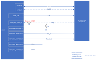
My design is compatible with QSPI or OSPI flash mounting:
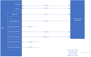
for flash QSPI, DS and loopback are not used :
for OSPI flash use DS connection :
Thank
Thomas,
Hi Thomas, I just assigned your query to a colleague that should be able to help you out shortly. Regards, Andreas
Hello Thomas Mongellaz
Thank you for the query.
Please refer some initial inputs i have:
- Is it possible to use OSPI0_LBCLKO/GPIO0_1 in GPIO mode?
The OSPI0_LBCLK0 has a uses case for the use of clock. It is recommended to consider this as a required clock signal and no configure for alternate function when used for OSPI interface
- The others pins OSPI0_CS1/GPIO0_12....OSPI0_CS3/GPIO0_14 can be used in GPIO mode if they are not used for OSPI fonction ?
You should be able to use the CS1..3 as GPIOs
OSPI0_DQS in GPIO mode ?
This is attached device and use case dependent.
if the attached device does not support DS, you should be able to use as GPIO.
Please note that this signal should not be routed toa attached device that has a DS function and then additionally used as a GPIO.
The functions need to be exclusive mutually.
I have reached out to other experts and will update if i hear anything additional from them.
Regards,
Sreenivasa
Hello Thomas Mongellaz
Please refer additional inputs i received from the expert:
the answer to these questions will depend on the timing modes they plan to use and the clocking topology required to support these modes. For example, the higher speed QSPI mode requires the external loopback clock topology and the higher speed OSPI mode requires the DQS clocking topology. They need to decide which clocking topologies are going to be supported before these questions can be answered.
Can you please add your inputs on the clocking topology you are considering and the required speed.
Regards,
Sreenivasa
Hello Sreenivasa,
Thank you for your reply.
We have three use cases on the same board :
1.Frist use case, the Device is a QSPI without DS and external loopback (clocking typology no loopback)
2. second use case, the device is a OSPI with a DS output which is not connected to DQS on the AM64 (clock typology no loopback)
3.third use case, the device is a OSPI with DS output which is connected to DQS on the AM64 (clocking typology DQS)
Regards,
Thomas MONGELLAZ
Hello Thomas Mongellaz
Thank you for the inputs.
Let me check with the team internally and update you.
regards,
Sreenivasa
Hello Thomas Mongellaz
Please refer to the TRM Bootmode section. Looks like the boot is configuring the below pin irrespective of the configuration.
Please let me know your thoughts.
Regards,
Sreenivasa
Hello Sreenivasa,
Thank for your reply.
In TRM :
in "AM64x and AM243x Schematic Review Checklist" documentation :
I read in the TRM that when using the no loopback mode, nothing should be connected to LBCLK. However DQS is not mentioned in the TRM. whereas in documentation "AM64x and AM243x Schematic Review Checklist" it is recommended to disconnect LBCLK and DQS.
To be sure when we do not use DQS, is it best to leave floating this input with no trace ?
If the DQS remains connected to a trace when not in use, can it cause functional issues?
Regards,
Thomas
Hello Thomas Mongellaz
Thank you.
To be sure when we do not use DQS, is it best to leave floating this input with no trace ?
If the DQS remains connected to a trace when not in use, can it cause functional issues?
When a trace is connected to the processor pads and not being actively driven, a parallel pull is recommended (pull polarity is customer use case dependent). During power-up, processor IO buffers are off and the IOs are in high impedance state (effectively an antenna that will pick up noise). Without any termination, these signals are very high impedance. This makes it easy for noise to couple energy on these floating signal trace and develop a potential that could exceed our recommended operating conditions, which would create an Electrical Over-Stress (EOS) on the IOs. ESD protection circuits inside the processor were only designed to protect the device from handling before being installed on a PCB assembly.
This behavior is not a concern when no trace is connected to the SOC pad and the default IO configurations are not modified.
Regards,
Sreenivasa
Hello Sreenivasa,
thank you for your reply.
My design :
Regards,
Thomas
Hello Thomas Mongellaz
Thank you.
The DQS is an SOC input. The 1K pulldown is required when a trace is connected to the SOC DQS pin nearest to the SOC.
A 0R should be placed near to the memory device to disconnect DQS to the SOC based on the use case.
If no trace is connected to the SOC DQS the need for pulldown does not arise.
Regards,
Sreenivasa