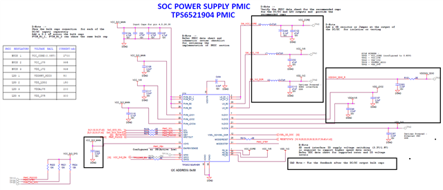
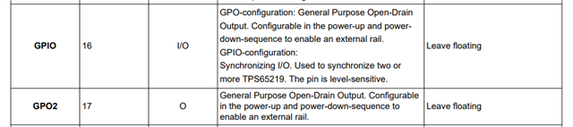
Other Parts Discussed in Thread: TPS65219, TPS6521905, TPS65215, AM2434, TPS65220, AM6421
Tool/software:
HI Board designers,
I am designing my board using TPS65219.
Are there some common recommendation or observations that i should be aware?
This thread has been locked.
If you have a related question, please click the "Ask a related question" button in the top right corner. The newly created question will be automatically linked to this question.
HI Board designers,
Refer below, common queries and replies
Q.1
Our customer has a question about TPS65219. Customer thinks to use TPS6521901 for supplying AM64x power. Is the TPS6521901 programmable device? Or, Is TPS6521901 not programmable device and customer cannot change anything of the output voltage and power sequence? If customer wants to change the power sequence, does customer needs to use TPS6521905? Customer worries about the unintentional change of power sequence. So, customer is happy if TPS6521901
The TPS6521901 and TPS6521905 both have NVM that can be reprogrammed. It is not easy to accidentally reprogram the NVM, so I do not think the customer needs to worry about accidentally modifying the power sequence.
The TPS6521905 comes with default setting with all outputs disabled, so it is helpful if a customer wants to program the device on the PCB while keeping all of the outputs in a safe state.
Q.2
Connecting the PMIC_LPM_EN0 to the PMIC MODE/STBY pin is optional. The TPS6521904 NVM has the MODE/STBY pin configured to select the Bucks switching mode with the following polarity:
If you are planning to use an AM62x low power mode where internal processor domains are turned-OFF while all the PMIC rails stay ON, then driving the MODE/STBY pin low with the PMIC_LPM_EN0 will allow to increase efficiency at light load.
Q.3
TPS6521908 is another option for customers who want to supply VDD_CORE with 0.85V instead of 0.75V. As noted in the processor datasheet, VDD_CORE and VDDR_CORE are expected to be powered by the same source so they ramp together when VDD_CORE is operating at 0.85V. In this scenario, we don't need to configure an LDO in the PMIC to supply 0.85 because Buck1 can supply both. This is why LDO2 is disabled.
Q.4
(+) TPS65219: 3.3V no output - Power management forum - Power management - TI E2E support forums
The TPS65219 PMIC executes two residual voltage checks; the first one occurs before the power-up sequence is executed and a second occurs during the power-up sequence (right before each rail is turned ON).
The first check can be disabled by changing register field "Register field "BYPASS_RAILS_DISCHA RGED_CHECK" but the second one cannot be disabled. Please note that changing any register field would require to turn-ON the PMIC first and get the device in Active state to enable I2C communication.
we found out where the residual voltage is coming from. This is come from E-PHY
- Residual voltage VLDO4 , 2.5V line : 4~500mV / VDDIO, 3.3V line : 50mV.
If the backfeeding issue on VLDO4 exist before the PMIC executes the power-up sequence, then none of the rails will turn-ON. The reason is because as I mentioned in my previous message, the PMIC performs the first residual voltage check before executing the power-up sequence.
Do you see a voltage on VLDO4 before Buck2 is turned ON?
TPS65219: Residual Voltage checks during start-up
Regards,
Sreenivasa
HI Board designers,
Refer additional inputs
Q.5
TPS6521905: NVM programing procedure
https://www.ti.com/lit/ug/slvucm5/slvucm5.pdf
Q.6
If the maximum output capacitance on the PMIC rails is exceeded, the phase margin starts to drop and stability gets affected.
Just for reference, the TPS65219 PMIC has an option for "multi-PMIC operation" that allows to fully synchronize the sequencing between multiple TPS65219 devices. This feature might help to split the load/POL capacitance across the PMIC rails. Is this a non-automotive application? The TPS65215 has a 4x4mm package option that helps to keep the overall power solution small even when using 2x TPS65219 devices.
This is a great feature in the TPS65219 PMIC that allows synchronizing multiple devices to power processors and SoCs that require multiple rails! Here is some information for the multi-PMIC operation, feel free to let us know if you have any questions and we will be happy to help.
Q.7 TPS65219: Share 3.3V rail for 2pcs AM2434 and peripherals
If the customer wants to use a single 3.3V rail to supply both MCUs and peripherals, then I would recommend using the TPS6521904 NVM instead.
Here are the two options when using TPS6521904:
Regards,
Sreenivasa
HI Board designers,
Refer additional inputs
Checklist and guidelines for PMIC
https://www.ti.com/lit/zip/slvafe2
Regards,
Sreenivasa
HI Board designers,
Refer below additional inputs:
TPS65219: Residual Voltage checks during start-up
ttps://e2e.ti.com/support/power-management-group/power-management/f/power-management-forum/1229202/tps65219-residual-voltage-checks-during-start-up
The TPS65219 PMIC performs a voltage check and discharge on each of its power rails to make sure they are all under the SCG threshold before executing the power-up sequence.
Although not recommended, this safety feature could be bypass by changing the register field "BYPASS_RAILS_DISCHARGED_CHECK" on address 0x1E. Since there is no I2C communication in Initialize state, PMIC would have to be programmed from factory to bypass the discharge check during power-up/power-down sequence. Any custom NVM configuration requires a new orderable part number and approval from our marketing team.
TPS65219: Programming NVM using the processor itself
TPS65219: Difference between TPS65219 and TPS65220
TPS65220 is designed to operate over extended temperature range.
Regards,
Sreenivasa
Hi Board designers
Input regarding selection of PMIC:
The recommend PMIC(s) on the product folder or used on the SK or EVM schematics has been designed considering the power sequencing, supply rail output slew, nRSTOUT (reset output) delay output from PMIC connected to MCU_PORz after all the supplies ramp for clock to be stable and the sizing of the supply rails based on the processor worst case current draw.
When choosing an alternate non-TI PMIC, the recommendation for custom board designers is to review the relevant collaterals including the data sheet and Maximum Current Ratings document and follow the requirements/recommendations. The recommendation is to review the slew rate requirements, Power-up and power-down sequence sections of the data sheet and confirm the non-TI PMIC based power architecture follows the recommendation.
An important point to note is the processor does not support dynamic scaling of the core voltage or the analog supplies.
Inputs regarding supply decay
Refer below FAQ
I have placed the note in both sections because it applies to both power-up and power-down. The power-up sequence should not begin until all power rails are below 300mV, and the power-down sequence is not complete until all power rails are below 300mV.
Regards,
Sreenivasa
HI Board designers,
Inputs on power supply sizing:
Using Maximum Current Ratings application note vs Power Estimation Tool PET
The max current app note is representing the current draw for a group of rails. Please note that it is not expected for this current to necessarily be replicated in the power estimation tool. The PET will tend to show more average use case power while the max current app note is intended to be used for power supply sizing as it will allow for the max transient on these groups with some margin. The PET should not be used for power supply sizing.
Regards,
Sreenivasa
HI Board designers,
Note:
How were these pdn specs derived? Is it based on worst case analysis?
Yes it is based on worst case load transient estimates for a given SoC design.
The Target impedance for AM62x and AM62xSiP will be identical as the same worst case load transients exist on both designs since they share the same die.
Via sharing recommendations in the escape application note are only made to help guide a customer to escape the design with fewer vias in the VCA regions. The number of vias used for escaping signals will ultimately depend on the specific customer use-case, the number of interfaces that need to be implemented and the layer count. If the specific use case allows the customer to use more vias for VDD_CORE in the VCA regions, that is definitely a valid approach. Per-pin loop inductance guidelines are more applicable for single-pin supplies that are connected to a decap. In case of multi-pin supplies like VDD_CORE where there are a number of parallel connections to multiple pins/decap thru multiple vias, it is hard to tie it back in to a per-pin requirement. The most important target to meet is the impedance target specified in Table 7-6 of the PDN Applications note. This table is the same for AM62x and AM62x SiP.
We do not include Buck output inductance in PDN simulations.
For VDDS_DDR: we do not recommend using target impedance as the signoff for DDR.
Refer to the AM62x, AM62Lx DDR Board Design and Layout Guidelines which outlines all details of power aware SI/PI simulations
that need to be run. The eye mask checks from these power aware simulations are the signoff.
Power Distribution Networks: Implementation and Analysis
Sitara Processor Power Distribution Networks: Implementation and Analysis
https://www.ti.com/lit/pdf/sprac76
Note: The decoupling capacitor numbers and type on the SK/EVM are only intended to serve as a guideline for customers. The true pass/fail criteria is the target impedance published in the PDN app note.
High Speed Board design and Signal integrity simulation
https://www.ti.com/lit/pdf/spraar7
https://www.ti.com/lit/pdf/spracn9
https://www.ti.com/lit/pdf/sprabi1
Inputs on PDN
Please refer below inputs i received:
Please note these are only recommendations and they need to contact their EDA vendor on what works best for their specific simulation environment.
1、Do I need to separate VDD_CORE-1 to 17 for simulation, or use VDD_CORE as a Port?
TI>> You can lump all VDD_CORE BGAs together as a single terminal for the port
2、Do I need to include the PMIC FB loop in the simulation?
TI>> If you are simulating only for AC impedance (target impedance checks) this is not required. The board layout from the inductor onwards (inductor not included) can be modeled and PMIC FB loop can be studied separately.
3、 Is the simulation starting frequency from 1Hz or from a minimum of 100kHz for the capacitor S2P?
TI>> There should be some DC frequency points added. Please check with your EDA vendor on the exact setup and simulation points needed to generate causal models.
I added additional inputs related to PDN and decoupling capacitors for reference.
The voltage at the device ball must never be below the MIN voltage or above the MAX voltage for any amount of time. This requirement includes dynamic voltage events such as AC ripple, voltage transients, voltage dips, and so forth
PCB design & Dcap scheme combine to form your board's Power Distribution Network (PDN) that should meet recommended SoC PI performance targets for robust processor operations. Each PCB design has a "unique finger-print" based upon component placements, power & Gnd routing, layer assignments, via qtys & locations, Dcap mounting & loop inductance, Dcap parameters, etc. As a result, an optimized Dcap scheme will vary from one PCB design to another but should provide a system PDN that meets PI performance targets when combined together. Similarly, the PI simulation tools can impact the estimated ZvsF response values, especially above 3.0MHz where non-3D extraction tools can return better Z values (10-15% less than more accurate 3D tools). This ican be due to a non-3D tool is only extracting a PCB's X & Y design elements & assuming a power & Gnd via inductances. Due to the 3D nature of current flow across & through a PCB from power & Gnd planes on different PCB layers, a 3D extraction gives a more accurate series inductance estimate needed to more accurately model power & Gnd vias which leads to a more accurate power rail impedance (ZvsF) response
it would be difficult to comment on reducing the amount of decoupling caps without going through the exercise ourselves. That said, you can likely prioritize the high-current and sensitive analog rails, then look to share bypass caps when you hit space constraints. Having decap as close to the BGA as possible will reduce inductance and improve their efficacy (two supply vias with a shared decap would be better than a decap located far away in most circumstances).
Please be aware that each PCB design is unique and may need different Dcap scheme to meet recommended PI parameter targets
Regarding decoupling capacitors, the recommendation is to start with the EVMs decoupling and then optimize (if needed) based on your power simulation results.
For the placement of the Caps and values, we would still recommend using the EVM as a reference along with the PDN document.
SK uses an EMI Filter at 1uF, can I replace it with a general ceramic capacitor?
The SK performance has been tested with 3-T terminal caps.
You may have to add multiple 2-T caps for each cap and perform simulations to finalize the values.
PDN application note
https://www.ti.com/lit/an/sprac76g/sprac76g.pdf
Regards,
Sreenivasa
Hi Board designers,
PMIC capacitor and feedback recommendations
PMIC - feed back and jumper or 0R provisioning
Regards,
Sreenivasa
Hi Board designers,
Refer below inputs for PMIC power sequencing.
AM6421: Sudden Loss of Power Impact on Power Down Sequence
As stated in the AM64x datasheet, "The potential applied to VDDR_CORE must never be greater than the potential applied to VDD_CORE + 0.18V during power-up or power-down. This requires VDD_CORE to ramp up before and ramp down after VDDR_CORE when VDD_CORE is operating at 0.75V". AM64 was characterized under operating conditions so we cannot guarantee the expected operation beyond the conditions specified in the datasheet. PCB designers are responsible for validating and characterizing the SoC under specific use case conditions to confirm it meets the application system level requirements.
Handling uncontrolled power-down requires additional considerations in the design like adding additional input capacitance or a discrete supervisor to monitor voltage at the power source and trigger an OFF request before PMIC loses power. Here is an example FAQ for reference: https://e2e.ti.com/blogs_/b/powerhouse/posts/how-to-meet-power-sequencing-requirements-with-a-pmic.
Another option to consider to mitigate the sequencing concerns during uncontrolled power-down is running the main CORE at 0.85V which allows to combine VDD_CORE and VDDR_CORE together. In this scenario both rails are supplied by the same PMIC DCDC regulator.
Regards,
Sreenivasa
Hi Board designers,
Information related to open drain GPO
Regards,
Sreenivasa