Other Parts Discussed in Thread: TDA4VM
Tool/software:
Questions about TDA4VM with DDR MT53E512M32D1ZW-046 AUT:B training:
1. By which register is TDA4VM configured for the internal DDR registers MR11, MR12, MR14 and MR22? Is the DDRSS_CTL_179 of the TDA4VM modifying the internal MR12 register of the DDR?
2. When is the command bus training, read DQ training, and write training of TDA4VM executed respectively? Does the TDA4VM automatically DDR train itself when the ambient temperature changes? Is dynamically adjusting refresh rate relevant to ddr training?
3. Will the MR11, MR12, MR14 and MR22 registers in the DDR be updated after command bus training, read DQ training and write training?
4. In the jacinto7 DDRSS regconfig tool, configure MR12 register CA VREF 25.6% (corresponding to 0x12 in DDR datasheet) in the DRAM IO configuration.
However, the code DDRSS_CTL_179 produced by tool is 0x27270056, and the corresponding percentage of 0x27 is 38.3%, which does not correspond to DDR datasheet. How to convert the value generated by tool and the value in DDR datasheet?
5. We measured different boards, and the reading value of DDRSS_CTL_179 is always 0x27270056 after starting up and after starting up for a period of time. This value also remains unchanged after the temperature changes (85°C to -40°C), and this value also remains unchanged after low temperature restart. When does DDR perform training?
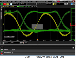
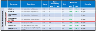
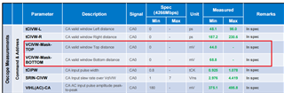
6. When Micron Laboratory helped us test the signal integrity, they reported that the MR12 and MR14 we provided were inaccurate, and the CA VREF they finally used was 20.5%, and the DQ VREF was 21.5%. And the test passed.
7. We have a board that will restart abnormally after running at a low temperature (-40℃) for a period of time, such as 2 hours, and it is normal at room temperature. May I ask how to capture log to help determine whether the restart is caused by abnormal DDR? The current log captured by the uart interface does not change before the restart.